(ZIF SSB)
(1.3, 2.3 & 5.7GHz)
(10GHz)
(3.4GHz)
(24GHz)
(HOME)
NO-TUNE SSB/CW TRANSCEIVER FOR 10GHz
Matjaz Vidmar, S53MV
1. Advantages and drawbacks of zero-IF transceivers
Zero-IF transceivers have both advantages and drawbacks when compared to conventional SSB transceivers with crystal filters and many frequency conversions. Considering the current state of technology, zero-IF transceivers are probably most suitable for the low amateur microwave bands: 1296MHz, 2304/2320MHz and 5760MHz. Therefore working radios for the above-mentioned frequency bands were developed first [1].
Although the published zero-IF transceivers for 1296MHz, 2304/2320MHz and 5760MHz allow many modifications and improvements of the original design, one would like to extend the zero-IF design to other frequency bands as well. However, the transfer of a transceiver design to another frequency band may not be straightforward.
Amateur-radio SSB transceivers for 432MHz and especially 144MHz require a very high dynamic range. A 144MHz SSB receiver should both withstand local stations with kilowatt transmitters as well as achieve a low noise figure. The dynamic range requirement for a 144MHz SSB receiver is probably even more demanding than for a HF (3-30MHz) receiver.
Extending the published 1296MHz SSB transceiver design to 432MHz or even to 144MHz does not make much sense. The dynamic range of the subharmonic mixers used in the 1296MHz RTX is certainly not sufficient for the current usage of the 144MHz amateur band. Due to several high-power stations, even direct AM demodulation in the simple subharmonic mixers would become a problem. A zero-IF SSB transceiver for 144MHz requires much better mixers operating at the fundamental LO frequency.
On the other hand it is not easy to find suitable components for very high frequencies. Only components for 10GHz (transistors, diodes etc) can be readily found on the market and it takes much effort to make them work on 24GHz. There are few parts suitable for 47GHz or higher frequencies. In addition, frequency accuracy, mixer balance and quadrature, mechanical stability and efficient shielding are more difficult to handle at higher frequencies.
In this article a zero-IF SSB transceiver for 10368MHz will be described. The design is based on the same components as the 5760MHz transceiver: HEMTs are used as amplifiers and BAT14-099R schottky quads are used as subharmonic mixers. Although 10GHz does not represent a problem for HEMTs yet, this seems to be the upper limit for the BAT14-099R quads. The BAT14-099R quads are packaged in the relatively large and unsymmetric SOT-143 package causing severe mixer unbalance problems.
The 10GHz SSB transceiver also includes PIN-diode antenna switching. The RF front-end is built on teflon laminate, while all other microstrip circuits are built on conventional FR4 glassfiber-epoxy, including several bandpass filters for 10GHz. The IF and AF sections are of course identical to those used in the transceivers for 1296, 2304 and 5760MHz.
2. Modified VCXO and multiplier stages
Although the radio-amateur 10GHz frequency-band allocation extends from 10000MHz to 10500MHz, most narrowband operation is concentrated slightly above 10368MHz. In the near future one may also expect narrowband activity in the satellite segment (10450-10500MHz), probably concentrated around the lower end around 10450MHz.
10368MHz is an integer multiple of many popular frequencies. For example, 10368MHz is the ninth harmonic of 1152MHz, a reference frequency that also generates 2304MHz, 3456MHz, 5760MHz and 24192MHz. 10368MHz is also the eighth harmonic of 1296MHz suggesting the use of the same VCXO and multiplier chain for 648MHz with some additional multiplier stages (X8) to obtain 5184MHz for the subharmonic mixers.
However, it makes sense to modify the VCXO itself for operation in the 10GHz transceiver. The relative crystal frequency pulling should be eight times smaller at 10GHz due to the additional multiplier stages. On the other hand, frequency stability is much more critical at 10368MHz than it is at 1296MHz.
Both requirements can be met by replacing the original VCXO using a 18MHz fundamental-resonance crystal with a modified VCXO using a 27MHz third-overtone crystal. Overtone crystals have a higher Q than fundamental crystals therefore providing better frequency stability. On the other hand, the frequency-pulling range of an overtone crystal is very restricted and it is barely sufficient for a 10GHz transceiver.
Fortunately the circuit diagrams of both VCXOs are similar and the same printed-circuit board can be used for both of them, including the multiplier chain up to 648MHz. Of course the 10GHz transceiver requires an additional multiplier for 5184MHz built in microstrip technology just like in the 5760MHz transceiver. The 648MHz input frequency is first multiplied by four to 2592MHz and then doubled to 5184MHz.
The modified VCXO and multiplier chain up to 648MHz are shown on Fig.1. A 27.000MHz crystal is required for operation at 10368MHz. The frequency-pulling range is very small in spite of the large capacitance ratio of the MV1404 varactor. The frequency coverage amounts to only 150-200kHz at the final frequency centered around 10368.100MHz.
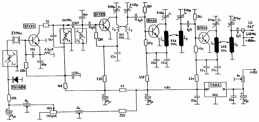
Fig.1 - VCXO and multipliers for 648MHz.
A coverage of 150kHz is however sufficient for normal 10GHz narrowband work, provided that the frequency stability is reasonable. Fortunately the 27.000MHz crystal is used in teletext decoders inside many TV sets. Thanks to very high volume production these inexpensive crystals have an excellent frequency stability.
The overtone oscillator itself (BFX89) is designed to reduce the loading and therefore the heating of the crystal, to further improve the frequency stability. The VCXO is followed by two resonant circuits (L2 and L3) tuned to 54MHz. The following multiplier stages are identical to those used in the 1296MHz transceiver and are tuned to 162MHz (X3), 324MHz (X2) and 648MHz (X2).
Since the VCXO module is followed by an additional multiplier for 5184MHz in the 10368MHz transceiver, an output power of 10mW (+10dBm) is sufficient at 648MHz. Therefore the power-supply resistors of the multiplier stages inside the VCXO module are increased to 330ohm, 330ohm and 220ohm. Since the printed-circuit board is the same as in the 1296MHz version and there are just a few minor variations in the component location, the corresponding drawings will not be published once again.
The circuit diagram of the additional multiplier for 5184MHz is shown on Fig.2. The circuit includes four HEMTs ATF35376. The first HEMT is overdriven by the 648MHz signal to produce many harmonics. The following microstrip bandpass (L3, L4, L5, L6, L7 and L8) selects the fourth harmonic at 2592MHz. The second HEMT amplifies the 2592MHz signal to drive the third HEMT operating as a frequency doubler. The doubler is followed by a 5184MHz bandpass (L15, L16, L17, L18, L19 and L20) and the 5184MHz signal is finally amplified by the last HEMT to obtain 20mW (+13dBm).
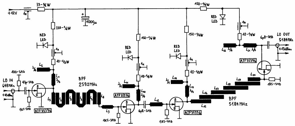
Fig.2 - Additional multiplier for 5184MHz.
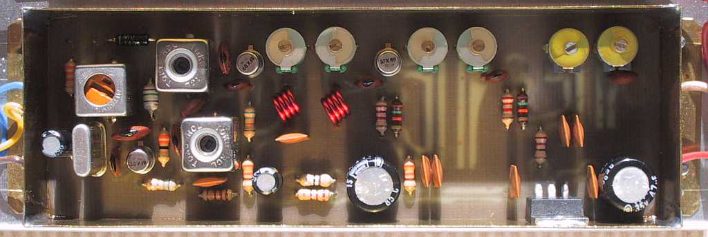
The additional multiplier for 5184MHz is built on a double-sided microstrip 0.8mm FR4 board with the dimensions of 20mmX120mm as shown on Fig.3. The corresponding component location is shown on Fig.4. The 5184MHz multiplier should provide the rated output power (+13dBm) without any tuning, provided that all of the components are installed and grounded correctly.
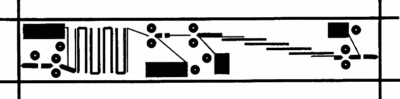
Fig.3 - 5184MHz multiplier PCB (0.8mm double-sided FR4).
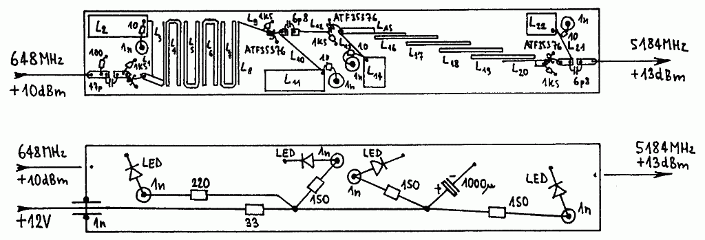
Fig.4 - 5184MHz multiplier component location.
3. Quadrature transmit mixer for 10368MHz
The circuit diagram of the quadrature transmit mixer for 10368MHz is shown on Fig.5. The 5184MHz LO signal is taken from a -15dB coupler and the LO signal level is restored by the ATF35376 amplifier stage, feeding two subharmonic mixers equipped with BAT14-099R schottky quads. The 5GHz lowpass attenuates the second harmonic at 10GHz to avoid corrupting the symmetry of the mixers.

Fig.5 - Quadrature transmit mixer for 10368MHz.
The unwanted carrier rejection of the BAT14-099R subharmonic mixers is only 10-15dB at 10368MHz. The main reason for the rather poor carrier rejection is the large and unsymmetrical SOT-143 package. Pin 1 of this SMD package is wider than the remaining three pins. Unfortunately, microwave schottky quads in suitable symmetric packages are hardly available and much more expensive than the BAT14-099R.
On the other hand, the subharmonic mixer balance can be corrected by a DC bias applied to the diodes. The quadrature transmit mixer for 10368MHz therefore includes two 10kohm trimmers to adjust the mixer balance. In this way the unwanted carrier rejection can be improved to better than 30dB.
The two 10GHz signals are combined in a quadrature hybrid. The hybrid is built as a 100ohm circuit to save board space. Quarter-wave transformers are used to restore the impedances to 50ohms. The circuit diagrams of both subharmonic mixers are slightly different from those used in the 1296, 2304 or 5760MHz versions for the same reason.
The hybrid is followed by a 10368MHz bandpass filter (L36, L37, L38, L39 and L40). The latter removes the 5184MHz LO as well as other unwanted mixing products. After filtering the 10368MHz SSB signal level is rather low (around 30uW or -15dBm), so two amplifier stages with ATF35376 HEMTs are used to boost the output signal level to about 2.5mW (+4dBm).
The quadrature transmit mixer for 10368MHz is built on a double-sided microstrip 0.8mm FR4 board with the dimensions of 30mmX120mm as shown on Fig.6. The corresponding component location is shown on Fig.7. Since only positive bias is available through the 10kohm trimmers for mixer balancing, the BAT14-099R packages should be oriented correctly in the circuit. In particular, one of the two packages has to be installed upside down.
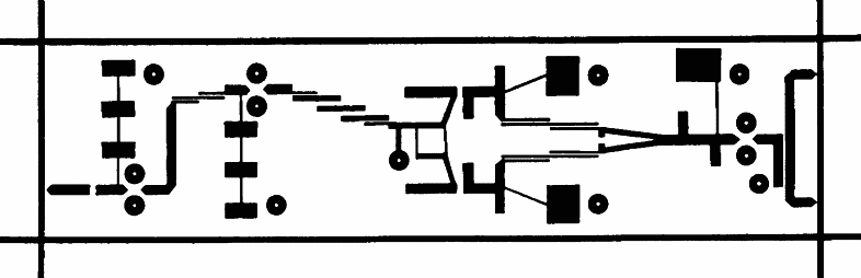
Fig.6 - 10368MHz TX mixer PCB (0.8mm double-sided FR4).
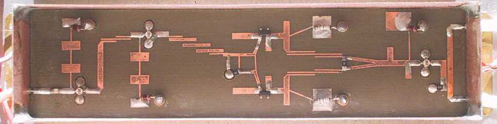
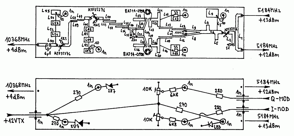
Fig.7 - 10368MHz TX mixer component location.
Except for the balancing trimmers, the quadrature transmit mixer for 10368MHz should not require any tuning. Both balancing trimmers are simply adjusted for the minimum output power when no modulation is present. This adjustment is best performed when the whole transceiver is assembled.
4. RF front-end for 10368MHz
The circuit diagram of the RF front-end for 10368MHz is shown on Fig.8. The RF front-end includes a transmit power amplifier, a receive low-noise amplifier and a PIN-diode antenna switch. Unlike the RF front-ends for 1296, 2304 or 5760MHz, all built on FR4 laminate, the RF front-end for 10368MHz is built as a microstrip circuit on 0.5mm thick teflon laminate to reduce RF losses.
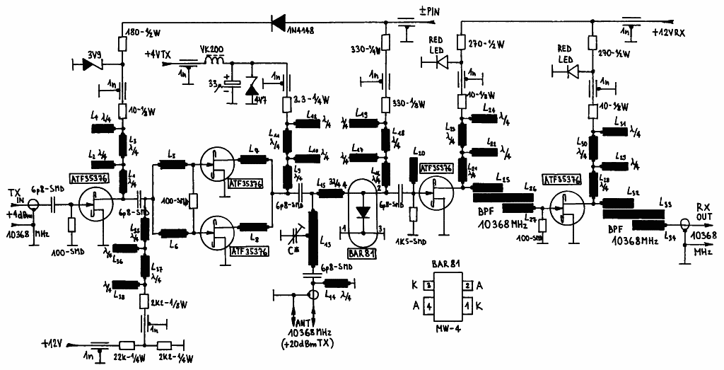
Fig.8 - RF front-end for 10368MHz.
Building the microstrip circuit on glassfiber-teflon laminate (thickness 0.5mm or 0.020", dielectric constant Er=2.55) allows an 1-2dB increase of the transmitter output power and an 1-2dB improvement of the receiver noise figure. The output power of the 10368MHz transmitter is in fact even slightly higher than the output power of the 5760MHz transmitter. Although both transmitters use the same semiconductor devices (HEMTs), the latter is built on lossy FR4 laminate.
The transmitter power amplifier is designed with inexpensive HEMTs, so the output power is limited to 100mW (+20dBm) on the antenna connector. The amplifier includes an ATF35376 HEMT driver stage followed by two ATF35376 HEMTs in parallel in the output stage. The 100ohm resistor between L5 and L6 improves the power dividing and prevents push-pull parasitic oscillations of the output stage.
The two output HEMTs receive a positive bias on the gates both while transmitting and while receiving. During transmission the transistors generate a self bias just like in the 5760MHz transmitter. Of course the +4VTX supply line requires a current-limiting resistor.
The antenna switch is using a single shunt PIN diode just like the 5760MHz counterpart with the PIN diode BAR80. However, the parasitic capacitance of the BAR80 is far too high for operation at 10368MHz, so the new diode BAR81 (SMD component marking "ABs" or "BBs", same MW-4 package) has to be used. The parasitic capacitance of the new BAR81 PIN diode is less than half that of the old BAR80. The insertion loss of the BAR81 is reduced by applying a negative bias (+-PIN) while receiving.
During transmission, the BAR81 is turned on and the short circuit is transformed by L15 into an open circuit at the summing node. The insertion loss of the BAR81 in the receive path exceeds 20dB and this is sufficient to protect the receiver. During reception, the two transmitter output HEMTs act as short circuits thanks to the positive gate bias. The short circuit is transformed through package parasitics, L7, L8 and interconnecting lines (total electrical length 3/4 lambda) into an open circuit at the summing node.
Since there are no strong signals expected in the 10GHz band, the LNA for 10368MHz includes two stages with ATF35376 HEMTs. The total insertion gain including the losses in the antenna switching network and the two 10368MHz bandpass filters amounts to about 23dB.
The RF front-end for 10368MHz is built on a double-sided microstrip 0.5mm glassfiber-teflon board with the dimensions of 30mmX80mm as shown on Fig.9. The corresponding component location is shown on Fig.10. A low-loss teflon laminate allows a higher output power and a better noise figure. On the other hand, a low-loss teflon laminate does not suppress the parasitic oscillations of HEMTs in the millimeter frequency range. These oscillations have to be controlled by damping resistors, usually 100ohm connected between gate and source.
Fig.9 - 10368MHz RF front-end PCB (0.5mm glassfiber-teflon Er=2.55).
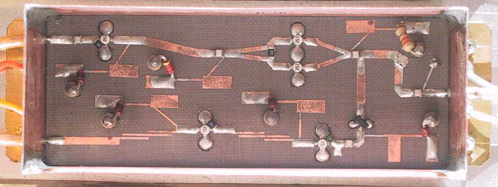
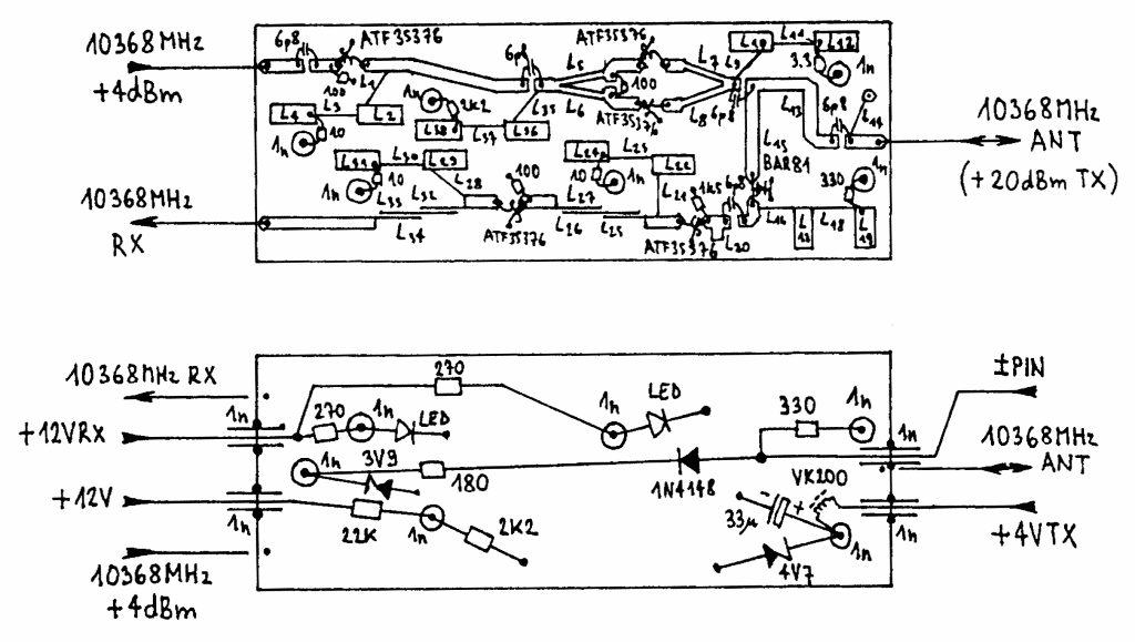
Fig.10 - 10368MHz RF front-end component location.
The RF front-end for 10368MHz includes a single tuning point. A capacitive tuning stub (a 2mmX3mm piece of copper foil) is added to L13 to improve the antenna matching, which in turn depends on the installation of the antenna cable and connector. This matching stub will improve the output power by about 1dB or in other words, the output power may be as low as 80mW without any tuning.
5. Quadrature receive mixer for 10368MHz
The circuit diagram of the quadrature receive mixer for 10368MHz is shown on Fig.11. It differs from the similar 5760MHz mixer in the design of the quadrature hybrid and subharmonic mixers with BAT14-099R diodes. The module includes two RF amplifiers with ATF35376 HEMTs, two 10368MHz bandpass filters, two subharmonic mixers operating in quadrature and two identical IF preamplifiers with BF199 transistors.
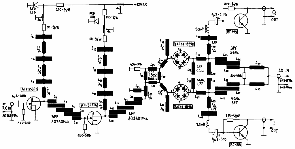
Fig.11 - Quadrature receive mixer for 10368MHz.
The subharmonic mixers are identical to those in the transmitter using BAT14-099R schottky quads. Both mixers are supplied in phase (L49 and L50) with the LO signal. The RF input signal is split by an 100ohm quadrature hybrid (L25, L26, L27 and L28). Impedance matching is provided by quarter-wavelength lines L23, L29 and L30.
The mixers are followed by two IF preamplifiers with BF199 transistors identical to those used in the 1296, 2304 and 5760MHz receivers. The 3.3mH chokes can be replaced by lower values, since powerful signals (both amateur and out-of-band) are not expected in the 10GHz band. Lower value chokes are less sensitive to disturbing low-frequency magnetic fields, including disturbing fields generated in the transceiver itself.
The quadrature receiving mixer for 10368MHz is built on a double-sided microstrip 0.8mm FR4 board with the dimensions of 30mmX120mm as shown on Fig.12. The corresponding component location is shown on Fig.13. In the 10GHz band, a quarter wavelength is only 4mm long on FR4 or 5mm long on teflon boards, so more complicated microstrip circuits can be used. For example, the supply/bias chokes are built as two-section lowpass filters on the RF-front-end teflon board and as three-section lowpass filters on both mixer FR4 boards. These improved RF chokes introduce less insertion loss and allow a lower crosstalk.
Fig.12 - 10368MHz RX mixer PCB (0.8mm double-sided FR4).
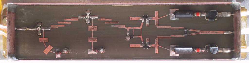
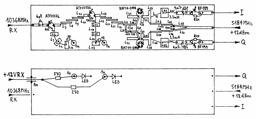
Fig.13 - 10368MHz RX mixer component location.
The receiving mixer for 10368MHz requires no tuning. However, the BF199 IF preamplifier transistors should be selected for the lowest noise. It seems that these transistors do not have a guaranteed "1/f" noise specification. In all of the prototypes built the Philips BF199 transistors produced the least amount of noise.
6. Construction of the zero-IF SSB transceiver for 10368MHz
The SSB/CW transceiver for 10368MHz is using the same quadrature modulator, IF amplifier and demodulator as the similar transceivers for 1296, 2304/2320 and 5760MHz. Since the same semiconductors are used as in the 5760MHz version, the current-limiting resistor in the SSB/CW switching RX/TX module has to be set to 82ohm, 1W.
The new PIN diode BAR81 also requires the small PIN driver module also used in the 5760MHz transceiver. Since the new BAR81 is much improved with respect to the old BAR80, the resulting receiver sensitivity loss amounts only to a few dB if no negative bias is provided (no PIN driver used) and the +-PIN line is simply connected to +12VTX. It therefore makes sense to use the new BAR81 also in the 5760MHz transceiver, while the old BAR80 is good enough for 1296 or 2304/2320MHz.
In the 10GHz frequency range, even small SMD components are rather large when compared to the wavelength of only 29mm. The size of the SMD resistors and capacitors is usually indicated in hundredths of an inch (0.254mm). The first SMD resistors and capacitors were of the size 1206 (about 3mmX1.5mm). Today, most SMD components are available in the sizes 0805 and 0603, while the newest components are of the size 0402 (dimensions 1mmX0.5mm).
Large 1206 SMD capacitors should not be used in the 10368MHz transceiver, since they have parasitic internal resonances in the 10GHz frequency range. The resonant frequencies are further decreased by the high dielectric constant of the ceramic used to build these capacitors. In the 10368MHz transceiver only 0805 or smaller SMD parts should be used.
In the 10GHz frequency range it makes sense to use small-value capacitors (mainly 6.8pF in the circuit diagrams), since they are built from low-loss WHITE ceramic with a moderate dielectric constant and internal resonances above 18GHz. Higher-value capacitors made from colored ceramic (purple or brown) have higher RF losses and lower resonance frequencies. Finally, the newest and smallest 0402 resistors and capacitors are useful even at 24GHz.
The main building block of the RF circuits operating at 10368MHz are the ATF35376 HEMTs, although there are many similar devices produced by other manufacturers that offer the same S-parameters at similar bias conditions. When selecting these devices one should take care of the Idss, since most of these transistors operate at zero bias for circuit
simplicity.
An Idss of about 30mA is desirable. Devices with higher Idss are only useful in the transmitter output amplifier. If devices with a sufficiently low Idss can not be obtained, then the 270-ohm 1/2W (or similar) resistors should be reduced to allow proper operation of the zener or LED shunt regulator. Lower NF selections of the same device, like the ATF35176 or the ATF35076, usually have a higher Idss!
The intermediate/audio frequency section of zero-IF or direct-conversion transceivers also requires a careful selection of active devices with low "1/f" of "popcorn" noise. Experience accumulated by building many transceivers for 1296, 2304/2320, 5760 and 10368MHz shows that Philips BF199 transistors perform best in the IF preamplifiers. However, several very noisy samples of the BC238 transistors had to be replaced in the quadrature IF amplifiers as well. It seems that factory rejects fairly exceeding the "1/f" noise requirements are sent to hobbyst shops. On the other hand, industrial leftovers found at flea markets perform best, since these devices had to go through severe input quality controls.
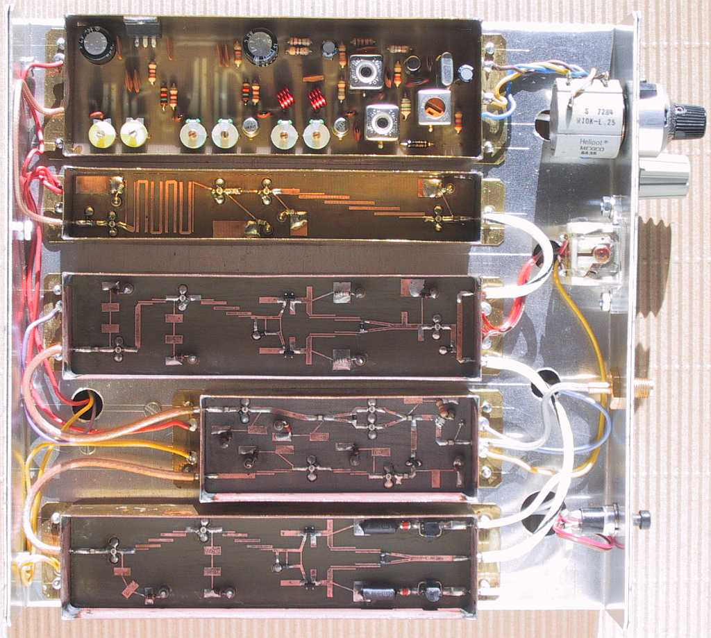
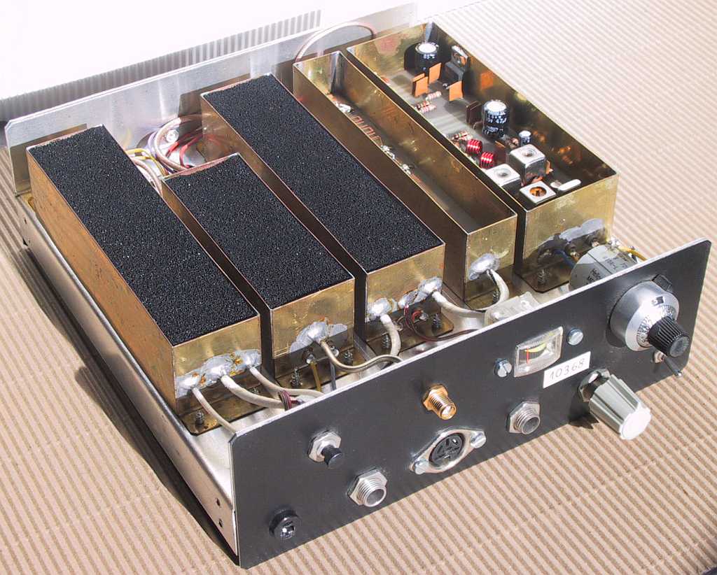
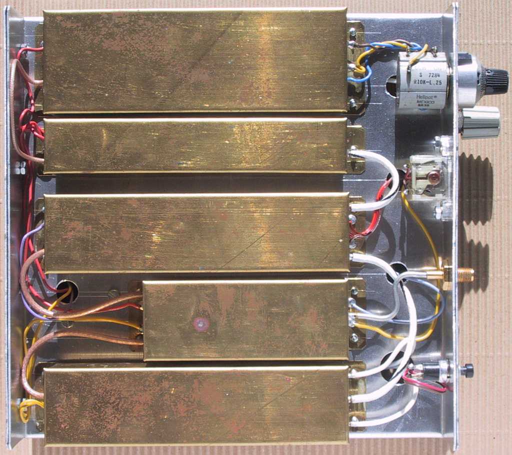
The RF modules of the 10368MHz SSB transceiver have the same dimensions as the corresponding units of the 5760MHz counterpart, but the exact locations of the electrical connections are slightly different. Their shielded enclosures should be carefully manufactured out of thin brass sheet, since the 10368MHz SSB transceiver is even more sensitive to microphonics and RF leakage. Both transmit and receive mixers and the RF front-end require 1cm thick microwave absorber foam (antistatic foam) installed under the covers of the shielded enclosures.
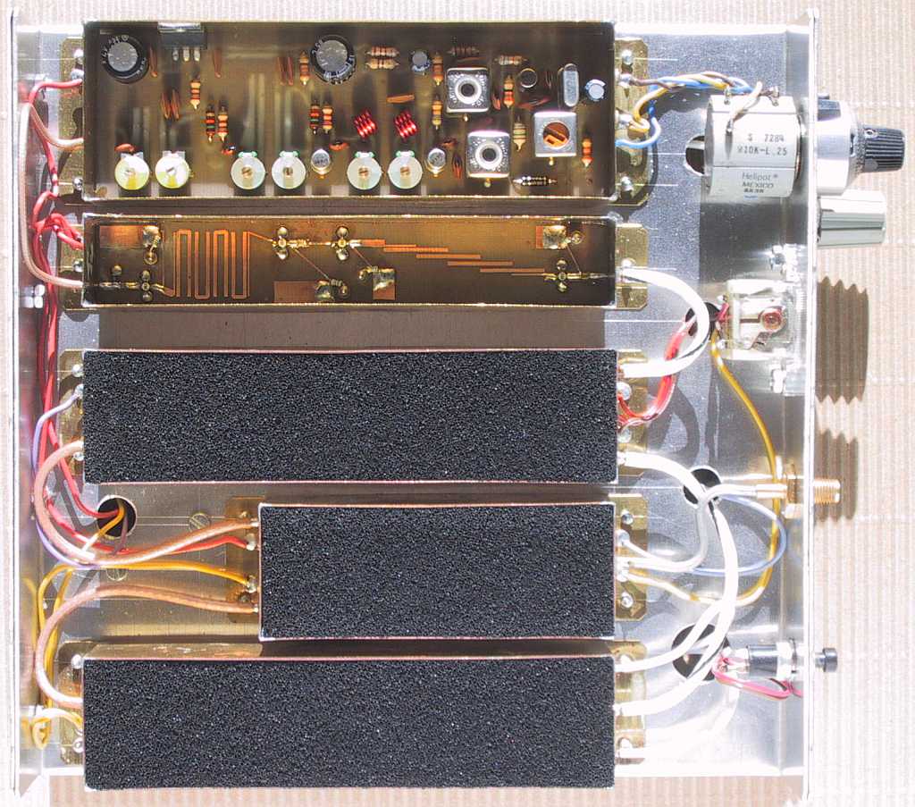
The VCXO module does not require a bottom cover like in the 1296MHz version, since 10368MHz is only the sixteenth harmonic of 648MHz. On the other hand, the additional multiplier for 5184MHz and the RF modules should be accurately shielded. Efficient feedthrough capacitors should be used elsewhere. All internal RF connections should be made with double-braid flexible teflon coax or UT085 semirigid.
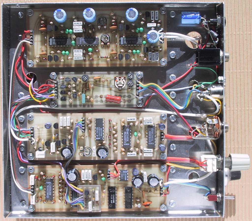
The complete 10368MHz SSB transceiver can be installed in the same enclosure as the 1296, 2304 or 5760MHz versions with a central chassis and internal dimensions of 60mm (height) X 180mm (width) X 180mm (depth). The module location within the enclosure is the same as in the 5760MHz version, including a similar wiring among the modules.
The loudspeaker should not be installed in the same case to avoid microphonics. Microphonics could perhaps be reduced by using machined enclosures for the RF modules. Mechanical vibrations can also be controlled by inserting pieces of plastic foam between the modules to act as an acoustic absorber.
7. Checkout of the zero-IF SSB transceiver for 10368MHz
The checkout of the transceiver should start with the alignment of the VCXO and multiplier stages. The VCXO should be adjusted for the desired frequency coverage. The multiplier stages are simply adjusted for the maximum output at the desired frequency. The maximum is observed as the rectified voltage drop on the base of the following transistor, measured through a suitable RF choke. The maximum on 648MHz is measured as the drain-current dip of the 2592MHz multiplier. Although the additional multiplier does not require any adjustments, the output signal level (+13dBm at 5184MHz) should be checked.
Since the receiver does not require any tuning, it should already work. First, the overall amplification should be checked. The output noise should drop when the supply to the LNA is removed. When the IF preamplifiers are disconnected, the noise should drop almost to zero.
Next the receiver is connected to an antenna and tuned to a weak unmodulated carrier (distant beacon etc). Besides the desired signal its rather weak image should also be heard in the loudspeaker. The image can be detected since its frequency changes in the opposite direction when tuning the receiver. The image is then attenuated by adjusting the two trimmers, phase quadrature and amplitude balance, in the IF amplifier.
The transmitter should be first checked for the output power. The full output power should be achieved with the trimmer in the modulator at about 1/3 resistance in CW mode. The DC voltage across the PA transistors should rise to the full voltage allowed by the 4V7 zener. Finally, the output power is optimized with the tuning stub on L13.
The transmitter is then switched to SSB to adjust the balance of both transmit mixers. The two 10kohm trimmers are simply adjusted for the minimum output power with no modulation. Unfortunately this setting is sensitive to the mixer-diode temperature and 5184MHz LO drive level, so the carrier suppression may not stay as good as it was adjusted during the checkout of the transceiver.
The SSB modulation should be checked in a radio contact with another amateur station on 10368MHz. In particular the correct sideband, USB or LSB, should be checked, since the I and Q modulation lines are easily interchanged by mistake. The other station should also check the carrier leakage or transmit mixer unbalance, heard as a 1365Hz tone added to the modulation.
Finally, the shielding of the transceiver should be checked. Waving your hand in front of the antenna usually causes a 1365Hz whistle in the loudspeaker of the receiver. The latter is caused by local oscillator leakage, frequency shifted by the Doppler effect of the moving hand and finally collected by the antenna. While this effect can not be eliminated completely with the suggested mechanical construction, it should be small enough to allow normal use of the transceiver. Of course, the receiver sensitivity and shielding can also be checked with a mains-operated fluorescent tube as described for the 1296, 2304 and 5760MHz transceivers.
The current drain of the described 10368MHz transceiver should be around 390mA during quiet reception at a nominal supply voltage of 12.6V. The current drain of the transmitter is inversely proportional to the output power and ranges from 550mA (CW or SSB peak power) up to 580mA (SSB no modulation). The current drain could be reduced substantially if a more efficient regulator were used to power the several HEMT stages with an operating voltage of only 2V.
* * * * *