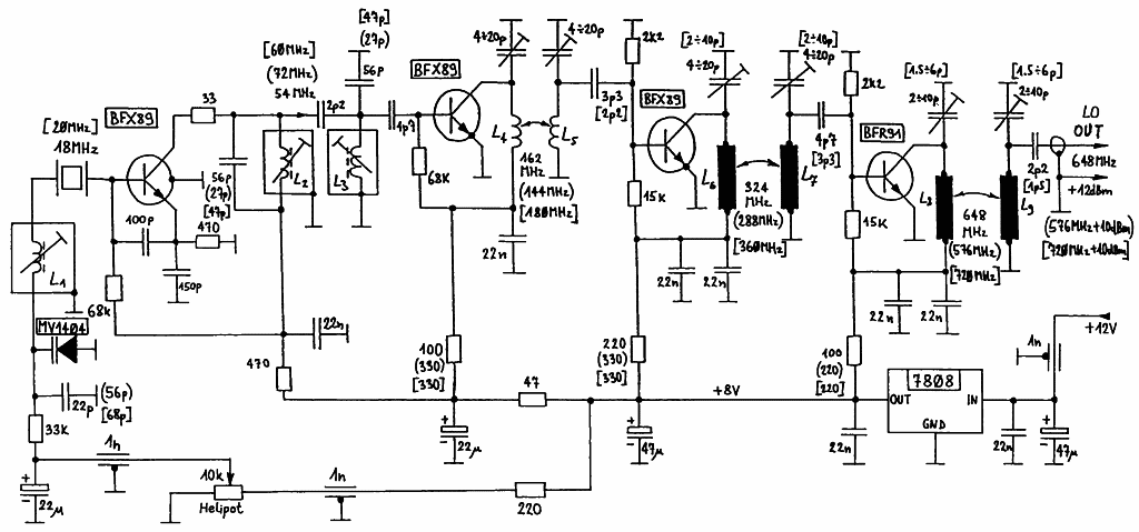
Fig.1 - VCXO and multipliers for 648MHz (576MHz) [720MHz].
(ZIF SSB)
(1.3, 2.3 & 5.7GHz)
(10GHz)
(3.4GHz)
(24GHz)
(HOME)
NO-TUNE SSB TRANSCEIVERS FOR 1296, 2304 & 5760MHz
Matjaz Vidmar, S53MV
1. Microwave SSB transceiver implementation
The described zero-IF concept should allow the design of simple and efficient SSB transceivers for an arbitrary frequency band. Three successful designs of zero-IF SSB transceivers covering the lower amateur microwave bands of 1296MHz, 2304MHz and 5760MHz will be described in this article. Similar technical solutions were first tested in PSK packet-radio transceivers operating at 1.2Mbit/s in the 23cm and 13cm amateur frequency bands.
The three zero-IF SSB transceivers for 1296MHz, 2304MHz and 5760MHz have many parts in common. In particular, the AF and IF sections are identical in all three transceivers. The RF sections are similar, however the microstrip filters are necessarily different as well as the low-noise and power devices used in each frequency band. Finally, the same VCXO module is used, with small modifications, in all three transceivers.
Therefore the individual modules will be described first. Of course, similar modules for different frequency ranges will be described together. Finally, an overview of the construction techniques of the individual modules will be given, as well as shielding of the modules and integration of the complete transceivers.
2. VCXO and multipliers
Since a relatively narrow frequency range needs to be covered, a VXO followed by multiplier stages is an efficient solution for the local oscillator. The VXO is built as a varactor-tuned VCXO with a fundamental-resonance crystal, since the frequency-pulling range of overtone crystals is not sufficient for this application. A fundamental-resonance crystal has a lower Q and is less stable than overtone crystals, but for this application the performance is sufficient.
Fundamental resonance crystals can be manufactured for frequencies up to about 25MHz. Therefore the output of the VCXO needs to be multiplied to obtain microwave frequencies. Frequency multiplication can be obtained by a chain of conventional multipliers including class-C amplifiers and bandpass filters or by a phase-locked loop.
Although the PLL requires almost no tuning and is easily reproducible, the PLL solution was discarded for other reasons. A SSB transceiver requires a very clean LO signal, therefore the PLL requires buffer stages to avoid pulling the VCXO and/or the microwave VCO. Shielding and power-supply regulation are also critical, making the whole PLL multiplier more complicated than a conventional multiplier chain.
The circuit diagram of the VCXO and multiplier stages is shown on Fig.1. The VCXO is operating around 18MHz in the transceivers for 1296MHz and 2304MHz and around 20MHz in the transceiver for 5760MHz. All multiplier stages use silicon bipolar transistors BFX89 (BFY90) except the last stage with a BFR91. The module already supplies the required frequency of 648MHz for the 1296MHz version of the transceiver.
Fig.1 - VCXO and multipliers for 648MHz (576MHz) [720MHz].
In the 2304MHz version, the module supplies 576MHz by using different multiplication factors. The latter frequency is doubled to 1152MHz inside the transmit and receive mixer modules. In the 5760MHz version, the module supplies 720MHz and this frequency is further multiplied to 2880MHz in an additional multiplier module. Of course, the values of a few components need to be adjusted according to the exact operating frequency, shown in () brackets for 2304MHz and in [] brackets for 5760MHz.
The VCXO and multiplier chain are built on a single-sided FR4 board with the dimensions of 40mmX120mm as shown on Fig.2. The corresponding component location (for the 648MHz version) is shown on Fig.3. The exact value of L1 depends on the crystal used. Some parallel-resonance crystals may even require replacing L1 with a capacitor. L2 and L3 have about 150nH each or 4 turns of 0.25mm copper-enameled wire on a 10X10mm IF-transformer coilformer. L4 and L5 are self-supporting coils of 4 turns of 1mm copper-enameled wire each, wound on an internal diameter of 4mm. L6, L7, L8 and L9 are etched on the PCB.

Fig.2 - VCXO PCB (0.8mm single-sided FR4).
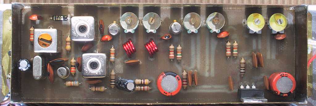
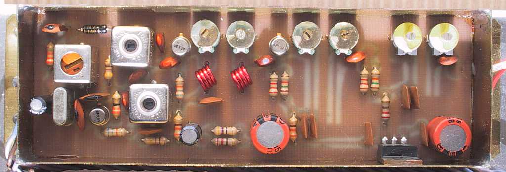
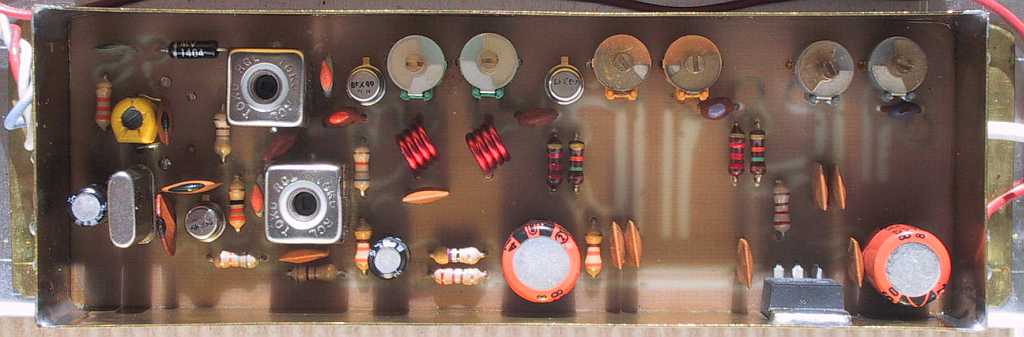

Fig.3 - VCXO component location (648MHz version).
The VCXO module is the only part of the whole transceiver that requires tuning. L2, L3 and the capacitors in parallel with L4, L5, L6, L7, L8 and L9 should simply be tuned for the maximum output at the desired frequencies. In a multiplier chain, RF signal levels can easily be checked by measuring the DC voltages over the BE junctions of the multiplier transistors.
When the multiplier chain is providing the specified output power, L1 and the capacitor in parallel with the MV1404 varactor should be set for the desired frequency coverage of the VCXO. If standard "computer grade" 18.000MHz or 20.000MHz crystals are used, it is recommended to select the crystal with the smallest temperature coefficient.
Unfortunately not all amateurs are allowed to use the international segment around 2304MHz on 13cm. It is a little bit more difficult to find a crystal for 18.125MHz for the German segment around 2320MHz.
The 5760MHz transceiver requires an additional multiplier from 720MHz to 2880MHz as shown on Fig.4. The first HEMT ATF35376 operates as a quadrupler while the second HEMT ATF35376 operates as a selective amplifier for the output frequency of 2880MHz. The additional multiplier for 2880MHz is built on a double-sided microstrip FR4 board with the dimensions of 20mmX120mm as shown on Fig.5. The corresponding component location is shown on Fig.6.
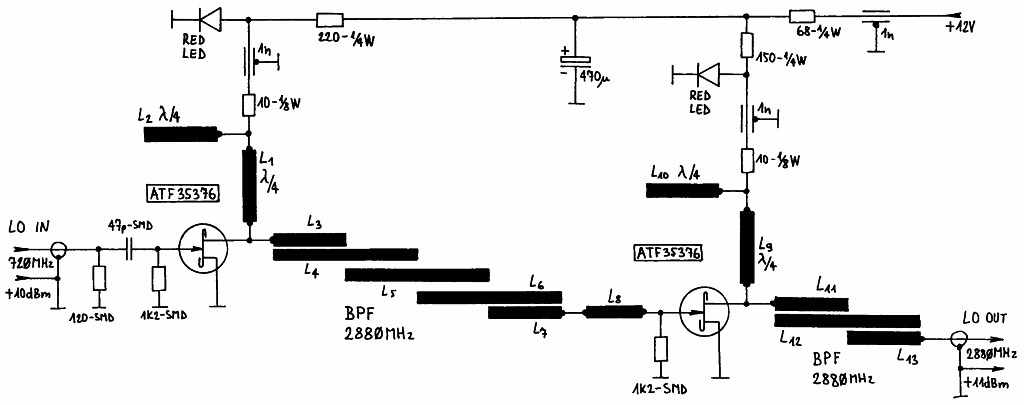
Fig.4 - Additional multiplier for 2880MHz.
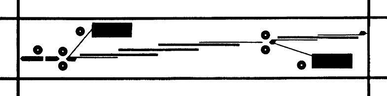
Fig.5 - 2880MHz multiplier PCB (0.8mm double-sided FR4).
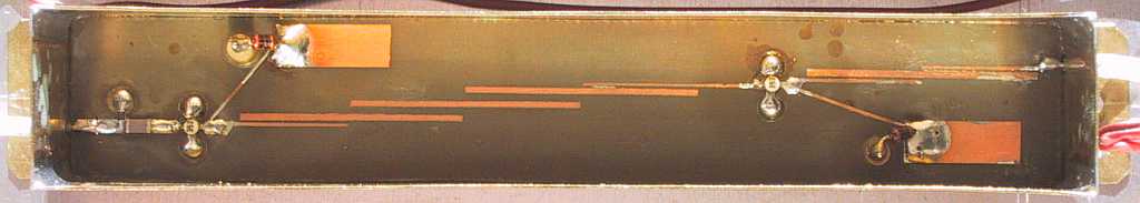
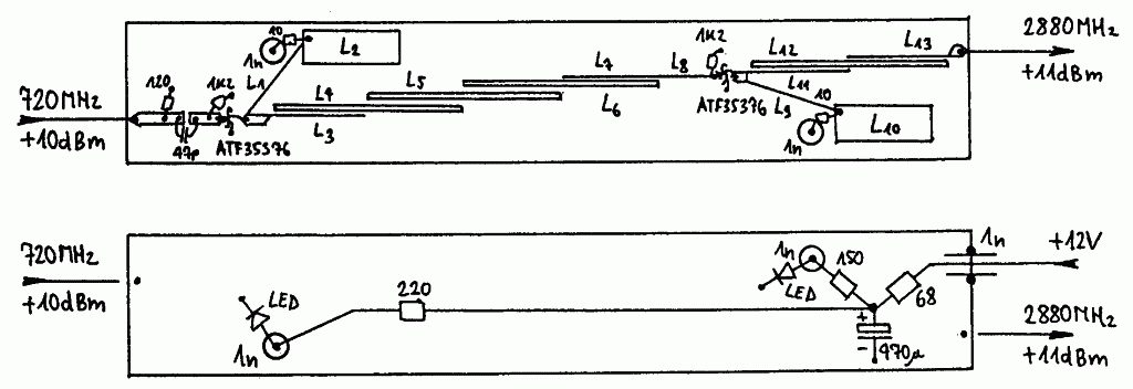
Fig.6 - 2880MHz multiplier component location.
The 2880MHz multiplier should provide the rated output power of +11dBm without any tuning. On the other hand, the tuning of L8 and L9 to 720MHz in the VCXO module can be optimized for the minimum DC drain current (max DC voltage) of the first HEMT. The two red LEDs are used as 2V zeners. LEDs are in fact better than real zeners, since they have a sharper knee and do not produce any avalanche noise.
3. SSB/CW quadrature modulator
The main purpose of the SSB/CW quadrature modulator is to convert the input audio frequency band from 200Hz to 2600Hz into two bands 0 to 1200Hz to drive the quadrature transmit mixer. Additionally the module includes a microphone amplifier and a circuit to generate the CW signal. The circuit diagram of the modulator module is shown on Fig.7.
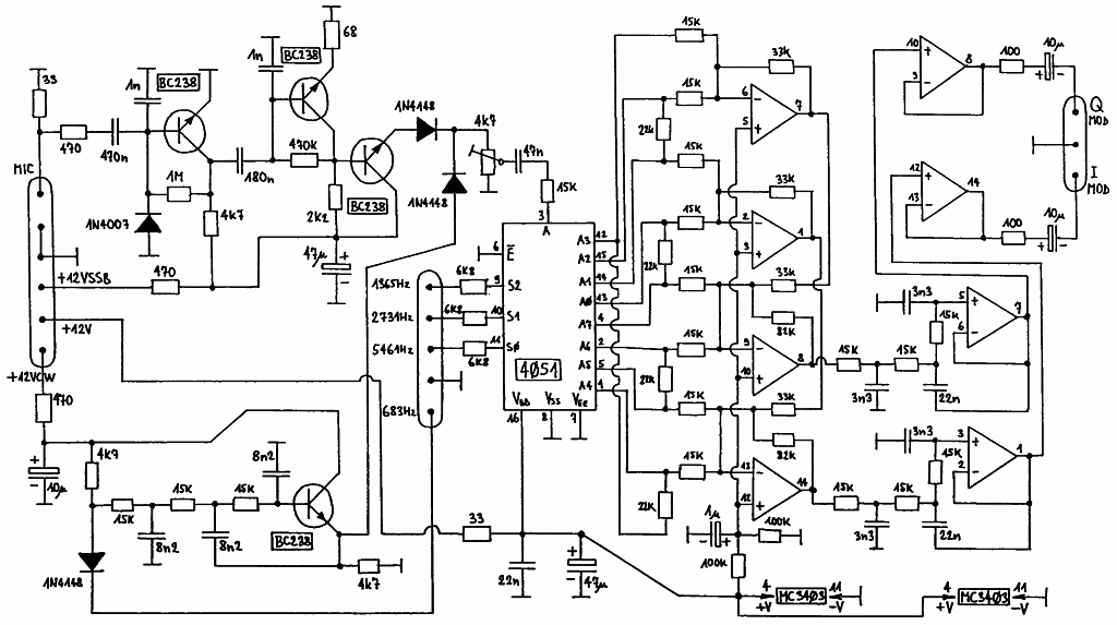
Fig.7 - SSB/CW quadrature modulator.
The microphone amplifier includes two stages with the transistors BC238. The input is matched to a low-impedance dynamic mike with the 33ohm resistor. The 1N4007 diode protects the input in the case the microphone input is simply connected in parallel to the loudspeaker output. Finally the output drives an emitter follower with another BC238.
The CW carrier is generated in the same way as the SSB transmission. The 683Hz square wave, coming from the demodulator module, is first cleaned in a low-pass audio filter and then processed in the same way as a SSB signal. Both AF modulation sources are simply switched by 1N4148 diodes.
The main component of the modulator is the 4051 CMOS analog switch. The switch is rotated with the 1365Hz, 2731Hz and 5461Hz clocks coming from the demodulator. The input audio signal is alternatively fed to the I and Q chains. The I and Q signals are obtained with a resistor network and the first four opamps (first MC3403). Then both I and Q signals go through lowpass filters to remove unwanted mixing products. Finally there are two voltage followers to drive the quadrature transmit mixer.
The SSB/CW quadrature modulator is built on a single-sided FR4 board with the dimensions of 40mmX120mm as shown on Fig.8. The corresponding component location is shown on Fig.9. Most components are installed vertically to save board space. The SSB/CW quadrature modulator does not require any alignment. The 4.7kohm trimmer is provided to check the overall transmitter. Full power (in CW mode) should be obtained with the trimmer cursor in central position.
Fig.8 - Modulator PCB (0.8mm single-sided FR4).
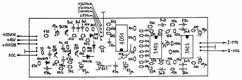
Fig.9 - Modulator component location.
4. Quadrature transmit mixers
All three transmit mixer modules for 1296MHz, 2304MHz and 5760MHz include similar stages: a LO signal switching, an in-phase LO divider, two balanced subharmonic mixers, a quadrature combiner and a selective RF amplifier. LO signal switching between the transmit and receive mixers is performed in the following way: most of the LO signal is always fed to the receive mixer. A small fraction of the LO signal is obtained from a coupler and amplified to drive the transmit mixer. During reception the power supply of the LO amplifier stage is simply turned off. This solution may look complicated, but in practice it allows an excellent isolation between the transmit and receive mixers. The practical circuit is simple and the component count is low as well.
The circuit diagram of the quadrature transmit mixer for
1296MHz is shown on Fig.10. The 648MHz LO signal is taken from a -20dB coupler and the LO signal level is restored by the BFP183 amplifier stage, feeding two subharmonic mixers equipped with BAT14-099R schottky quads. The 648MHz lowpass attenuates the second harmonic at 1296MHz to avoid corrupting the symmetry of the mixers.
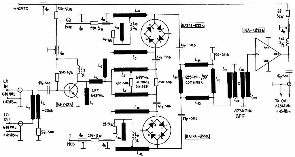
Fig.10 - Quadrature transmit mixer for 1296MHz.
The two 1296MHz signals are combined in a quadrature hybrid, followed by a 1296MHz bandpass filter. The latter removes the 648MHz LO as well as other unwanted mixing products. After filtering the 1296MHz SSB signal level is rather low (around -10dBm), so an INA-10386 MMIC is used to boost the output signal level to about +15dBm.
The quadrature transmit mixer for 1296MHz is built on a double-sided microstrip FR4 board with the dimensions of 40mmX120mm as shown on Fig.11. The corresponding component location is shown on Fig.12. The circuit does not require any tuning for operation at 1296MHz or 1270MHz.
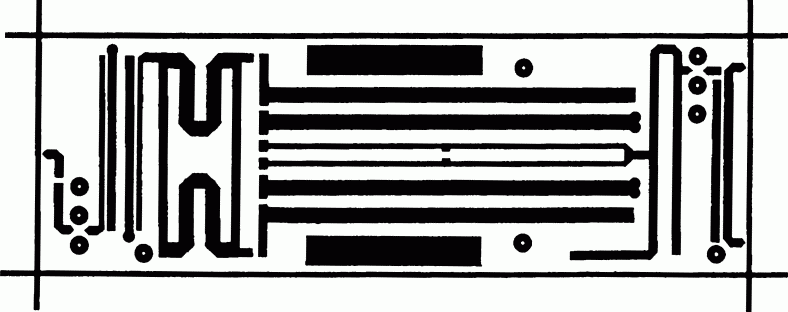
Fig.11 - 1296MHz TX mixer PCB (0.8mm double-sided FR4).
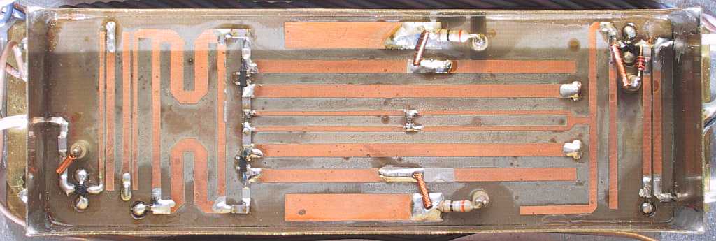
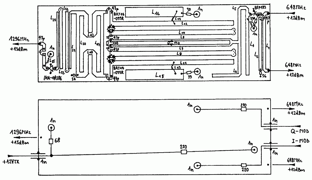
Fig.12 - 1296MHz TX mixer component location.
The circuit diagram of the quadrature transmit mixer for 2304MHz is shown on Fig.13. The 576MHz LO signal is taken from a -20dB coupler, amplified by the BFP183 transistor and then doubled to 1152MHz by the BFP196 transistor. The doubler output goes through a microstrip bandpass filter to feed the two subharmonic mixers with BAT14-099R schottky quads.
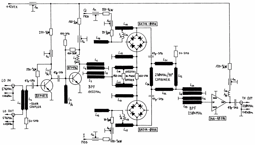
Fig.13 - Quadrature transmit mixer for 2304MHz.
The two 2304MHz signals are combined in a quadrature hybrid, followed by a 2304MHz bandpass filter. The latter removes the 1152MHz LO as well as other unwanted mixing products. After filtering the 2304MHz SSB signal level is rather low (around -11dBm), so an INA-10386 MMIC is used to boost the output signal level to about +10dBm.
The quadrature transmit mixer for 2304MHz is built on a double-sided microstrip FR4 board with the dimensions of 40mmX120mm as shown on Fig.14. The corresponding component location is shown on Fig.15. The circuit does not require any tuning for operation at 2304MHz or 2320MHz. For operation in the satellite band above 2400MHz, the LO bandpass should be readjusted to 1200MHz by shortening L7 and L8 at their hot ends.
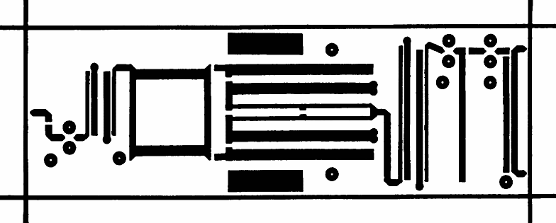
Fig.14 - 2304MHz TX mixer PCB (0.8mm double-sided FR4).
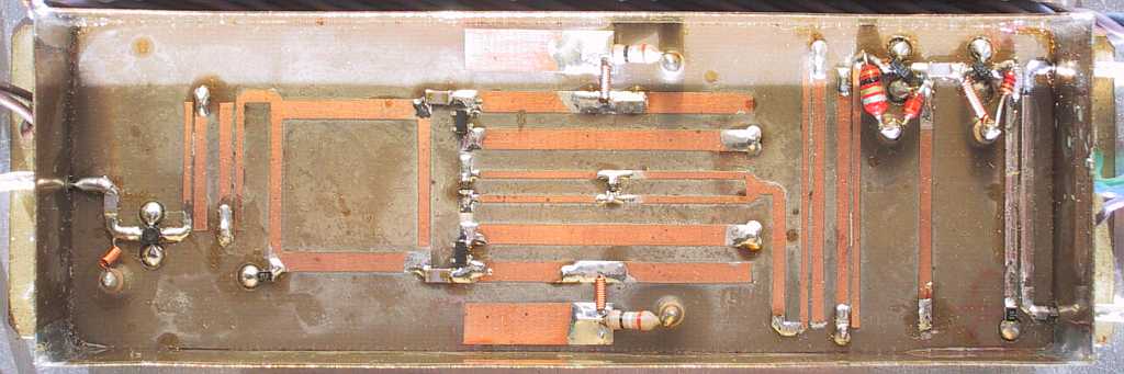
Fig.15 - 2304MHz TX mixer component location.
The circuit diagram of the quadrature transmit mixer for 5760MHz is shown on Fig.16. The 2880MHz LO signal is taken from a -15dB coupler and the LO signal level is restored by the ATF35376 amplifier stage, feeding two subharmonic mixers equipped with BAT14-099R schottky quads. The 2880MHz lowpass attenuates the second harmonic at 5760MHz to avoid corrupting the symmetry of the mixers.
Fig.16 - Quadrature transmit mixer for 5760MHz.
The two 5760MHz signals are combined in a quadrature hybrid, followed by a 5760MHz bandpass filter. The latter removes the 2880MHz LO as well as other unwanted mixing products. After filtering the 5760MHz SSB signal level is rather low (around -14dBm), so two amplifier stages with ATF35376 HEMTs are used to boost the output signal level to about +11dBm.
The quadrature transmit mixer for 5760MHz is built on a double-sided microstrip FR4 board with the dimensions of 30mmX120mm as shown on Fig.17. The corresponding component location is shown on Fig.18. The circuit does not require any tuning for operation at 5760MHz.
Fig.17 - 5760MHz TX mixer PCB (0.8mm double-sided FR4).
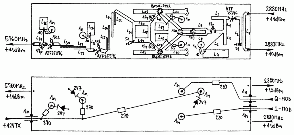
Fig.18 - 5760MHz TX mixer component location.
The quadrature transmit mixers do not supply any output signal when the modulation input is absent. For transmitter testing purposes it is possible to obtain an output signal by feeding a DC current of 2-10mA into one or both mixers.
5. RF front-ends
The RF front-ends include the transmitter power amplifiers, the receiver low-noise amplifiers and the antenna switching circuits. Of course there are major differences among different power amplifier designs, depending not just on the frequency, but also on the technology used and the output power desired. On the other hand, it no longer makes sense to use expensive coaxial relays, since PIN diodes can provide the same insertion loss and isolation at lower cost with better reliability and much shorter switching times.
The circuit diagram of the RF front-end for 1296MHz is shown on Fig.19. The transmitter power amplifier includes a single stage with a CLY5 power GaAsFET, providing a gain of 15dB and an output power of about 1W (+30dBm). The CLY5 is a low-voltage transistor operating at about 5V.
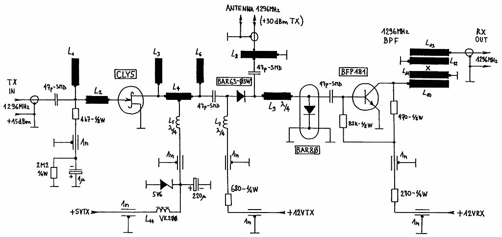
Fig.19 - RF front-end for 1296MHz.
The negative gate bias is generated by rectification of the driving RF signal in the GS junction inside the CLY5 during modulation peaks. The gate is then held negative for a few seconds thanks to the 1uF storage capacitor. To prevent overheating and destruction of the CLY5, the +5VTX voltage is obtained through a current-limiting resistor. This arrangement may look strange, but it is very simple, requires no adjustments, allows a reasonably linear operation and most important of all, it proved very reliable in PSK packet-radio transceivers operating 24 hours per day in our packet-radio network.
The antenna switch includes a series diode BAR63-03W and a shunt diode BAR80. Both diodes are turned on while transmitting. L9 is a quarter-wavelength line that transforms the BAR80 short circuit into an open for the transmitter. The receiving preamplifier includes a single BFP181 transistor (15dB gain) followed by a 1296MHz bandpass filter (-3dB loss). In the 1296MHz RF front-end, the LNA gain should be limited to avoid interference from powerful non-amateur users of this band (radars and other radionavigation aids).
The RF front-end for 1296MHz is built on a double-sided microstrip FR4 board with the dimensions of 40mmX80mm as shown on Fig.20. The corresponding component location is shown on Fig.21. The RF front end for 1296MHz requires no tuning. However, since the output impedance of the INA-10386 inside the transmit mixer is not exactly 50ohms, the cable length between the transmit mixer and the RF front-end is critical. Therefore L1 may need adjustments if the teflon-dielectric cable length is different from 12.5cm.
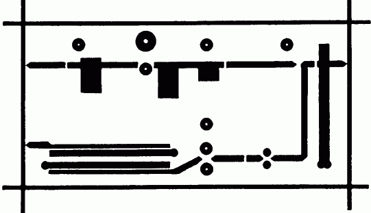
Fig.20 - 1296MHz RF front-end PCB (0.8mm double-sided FR4).
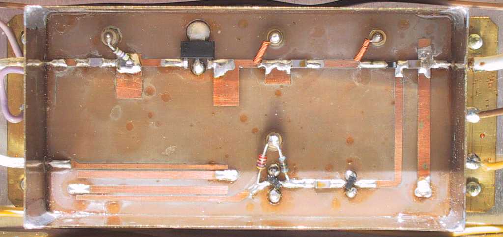
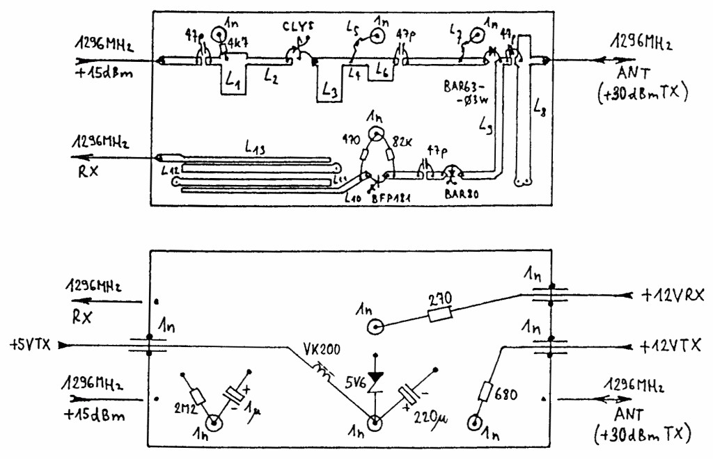
Fig.21 - 1296MHz RF front-end component location.
The circuit diagram of the RF front-end for 2304MHz is shown on Fig.22. The transmitter power amplifier includes two stages: a BFP183 driver and a CLY2 final amplifier. The additional BFP183 driver is required since the gain and output power of the INA-10386 inside the transmit mixer are smaller at 2304MHz than at 1296MHz. Further the additional bandpass filter at the input of the power amplifier adds some insertion loss.
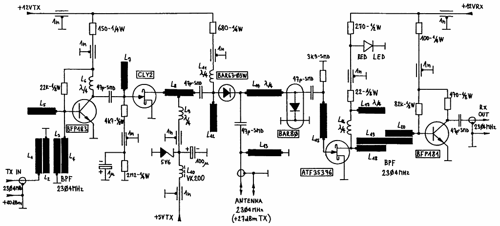
Fig.22 - RF front-end for 2304MHz.
The BFP183 operates as a class-A amplifier while the CLY2 is used in a similar self-biasing arrangement like the CLY5 in the 1296MHz front-end. Of course the drain current of the CLY2 is smaller, the +5VTX current-limiting resistor must be higher and the RF output power on the antenna connector amounts to about 0.5W (+27dBm). The PIN-diode antenna switch is identical to that used in the 1296MHz RF front-end with a series diode BAR63-03W and a shunt diode BAR80.
Since there are no powerful users of the 2.3GHz band, the RF front-end for 2304MHz includes a two-stage LNA: a HEMT ATF35376 in the first stage and a BFP181 in the second stage. The overall gain of the LNA is around 23dB. Since the Idss of the ATF35376 is usually around 30mA, no negative voltage needs to be applied to the gate.
The RF front-end for 2304MHz is built on a double-sided microstrip FR4 board with the dimensions of 40mmX80mm as shown on Fig.23. The corresponding component location is shown on Fig.24. The RF front-end for 2304MHz should require no tuning, since both the transmit and the receive chains have a few dB of gain margin. However, in order to squeeze the last milliwatt out of the CLY2 (is it really necessary?), some tuning may be attempted on the output.
Fig.23 - 2304MHz RF front-end PCB (0.8mm double-sided FR4).
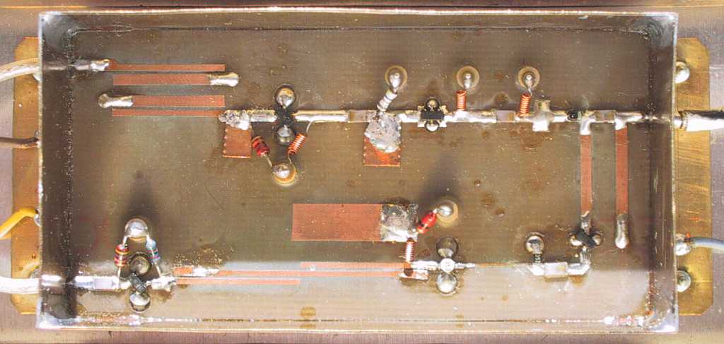
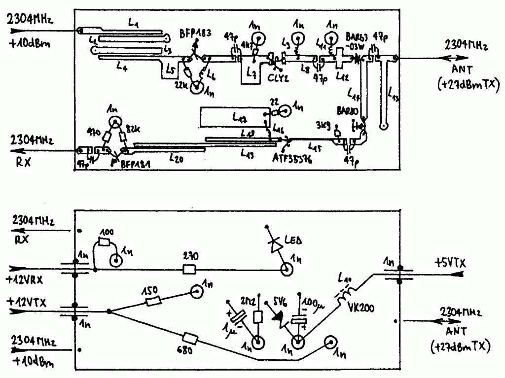
Fig.24 - 2304MHz RF front-end component location.
The circuit diagram of the RF front-end for 5760MHz is shown on Fig.25. The transmit power amplifier uses two HEMTs ATF35376 in parallel to obtain about 100mW (+20dBm) on the antenna connector. The gain of the HEMTs is around 13dB, however circuit losses both in the input matching network and in the antenna switch on the output amount to about 3dB, so that about +10dBm of drive power is required.
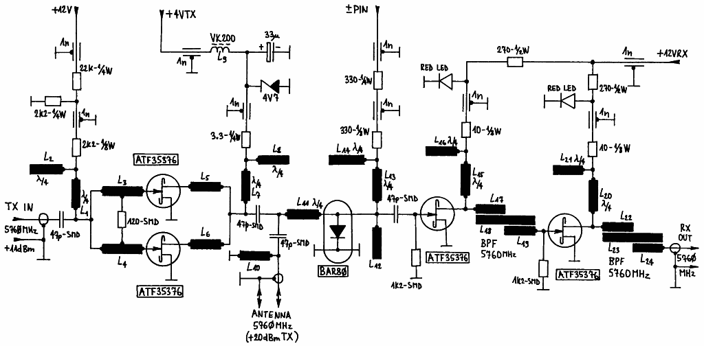
Fig.25 - RF front-end for 5760MHz.
The two PA HEMTs receive a positive bias on the gates both while transmitting and while receiving. In transmission the PA HEMTs generate a self bias just like the CLY5 and CLY2 power GaAsFETs. Of course the +4VTX supply line requires a current-limiting resistor.
The antenna switch includes a single shunt diode BAR80 to protect the receiver input during transmission. During reception, the two PA HEMTs act as short circuits thanks to the positive gate bias. The short circuit is transformed through package parasitics, L5, L6 and interconnecting lines (total electrical length 3/4 lambda) into an open circuit at the summing node.
Since the shunt diode BAR80 was not designed for operation above 3GHz, its capacitance introduces additional insertion loss in the receiving path at 5.76GHz. This additional loss can be substantially reduced if a reverse bias is applied to the BAR80 diode. Therefore a negative bias voltage is applied to the BAR80 during reception and a positive current is applied during transmission through the command line +-PIN.
Since there are no strong signals expected in the 5.7GHz band, the LNA for 5760MHz includes two stages with ATF35376 HEMTs. The total insertion gain including the losses in the antenna switching network and the two 5760MHz bandpass filters amounts to about 23dB.
The RF front-end for 5760MHz is built on a double-sided microstrip FR4 board with the dimensions of 30mmX80mm as shown on Fig.26. The corresponding component location is shown on Fig.27. The RF front-end for 5760MHz requires no tuning. It is however recommended to select the ATF35376 HEMTs according to the Idss. The highest Idss devices should be used in the transmitter PA while the lowest Idss devices should be used in the receiver LNA.

Fig.26 - 5760MHz RF front-end PCB (0.8mm double-sided FR4).
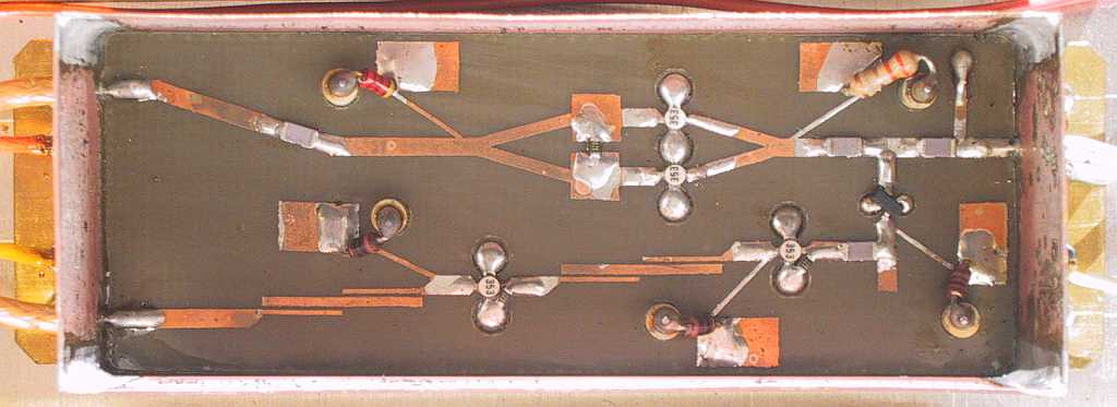
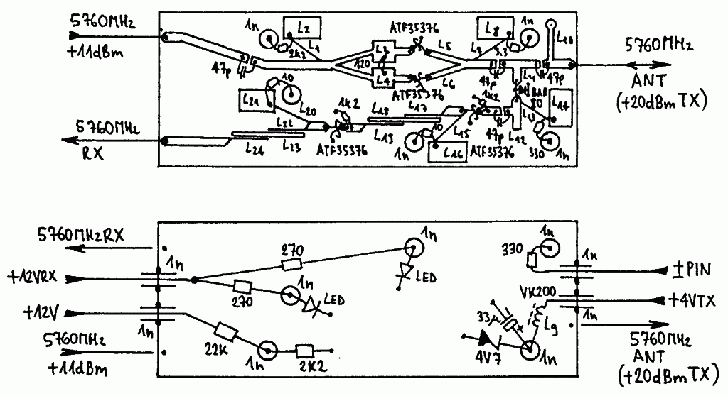
Fig.27 - 5760MHz RF front-end component location.
6. Quadrature receive mixers
All three receiving mixer modules for 1296MHz, 2304MHz and 5760MHz include similar stages: an additional RF signal amplifier, a quadrature-hybrid divider, two subharmonic mixers, an in-phase LO divider and two IF preamplifiers. The mixers, in-phase and quadrature dividers and RF bandpass filters are very similar to those used in the transmitting mixer modules.
The circuit diagram of the quadrature receiving mixer for 1296MHz is shown on Fig.28. The incoming RF signal is first fed through a microstrip bandpass filter, then amplified with an INA-03184 MMIC and further filtered by another, identical microstrip bandpass. The total gain of the chain of the two filters and the MMIC is about 20dB.
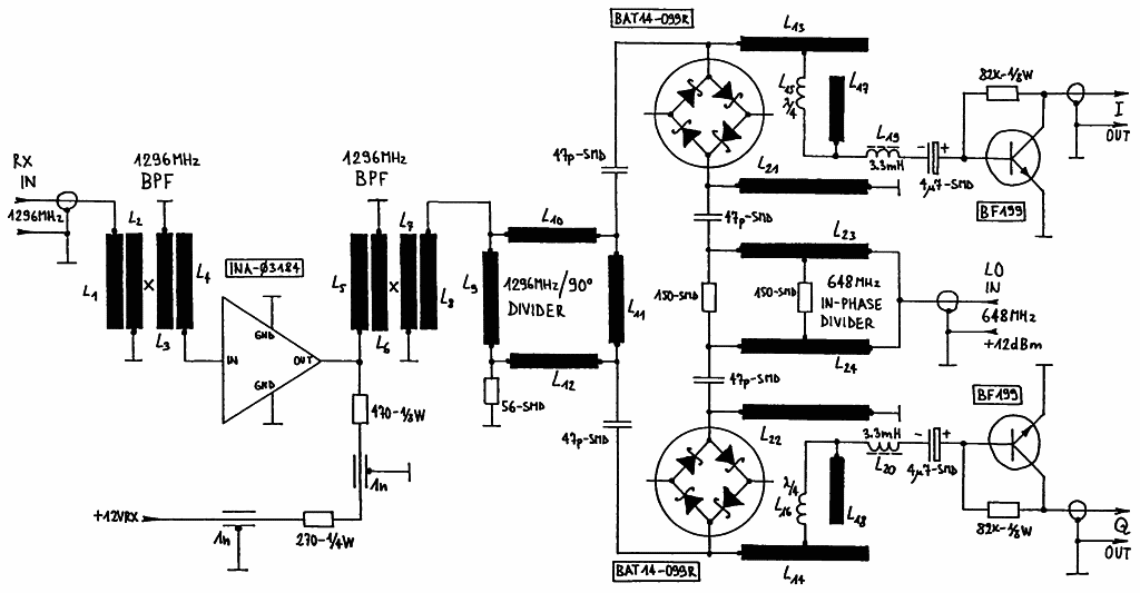
Fig.28 - Quadrature receive mixer for 1296MHz.
A high gain in the RF section is required to cover the relatively high noise figure of the two subharmonic mixers and the additional losses in the quadrature hybrid. The two receiving subharmonic mixers are also using BAT14-099R schottky quads. The mixer outputs are fed through lowpass filters to the IF preamplifiers.
The IF preamplifiers are using HF transistors BF199. These were found to perform better than their BC... counterparts in spite of the very low frequencies involved (less than 1200Hz). HF transistors have a smaller current gain, their input impedance is therefore smaller and better matches the output impedance of the mixers. Both IF preamplifiers receive their supply voltages from the IF amplifier module.
The quadrature receiving mixer for 1296MHz is built on a double-sided microstrip FR4 board with the dimensions of 40mmX120mm as shown on Fig.29. The corresponding component location as shown on Fig.30. The receiving mixer for 1296MHz requires no tuning.
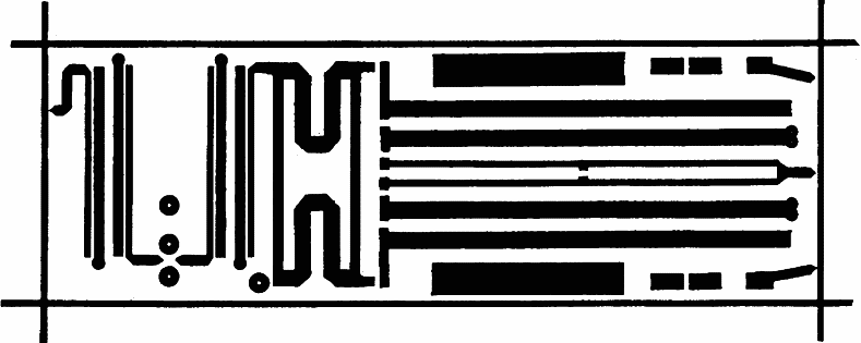
Fig.29 - 1296MHz RX mixer PCB (0.8mm double-sided FR4).
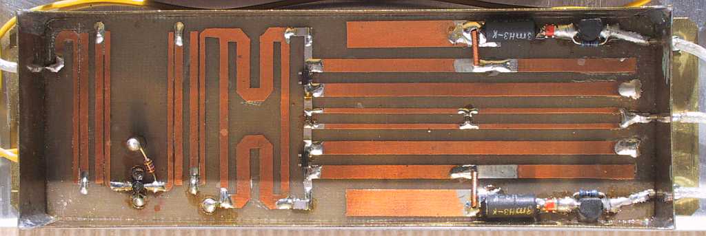

Fig.30 - 1296MHz RX mixer component location.
The circuit diagram of the quadrature receiving mixer for 2340MHz is shown on Fig.31. Since the same components, INA-03184 MMIC and BAT14-099R schottky quads, have similar performances in the 1296MHz and 2304MHz frequency bands, the circuit diagram of the 2304MHz mixer is almost identical to the 1296MHz mixer.
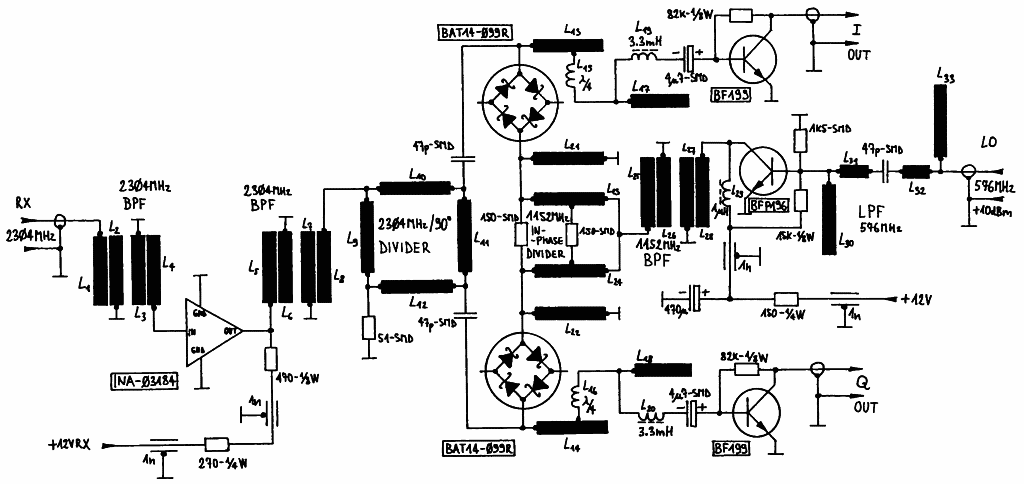
Fig.31 - Quadrature receive mixer for 2304MHz.
The only difference is the additional frequency doubler to 1152MHz with the transistor BFP196. The multiplier includes a lowpass on the input and a bandpass filter on the output. The input lowpass filter should prevent unwanted interactions with other circuits operating with the same 576MHz LO signal. The 1uH choke should have a ferrite core for the same reason.
The quadrature receiving mixer for 2304MHz is built on a double-sided microstrip FR4 board with the dimensions of 40mmX120mm as shown on Fig.32. The corresponding component location is shown on Fig.33. The receiving mixer does not require any tuning for operation on 2304MHz or 2320MHz. For operation in the satellite band above 2400MHz, the LO bandpass should be readjusted to 1200MHz by shortening L26 and L27 at their hot ends.

Fig.32 - 2304MHz RX mixer PCB (0.8mm double-sided FR4).
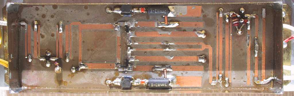
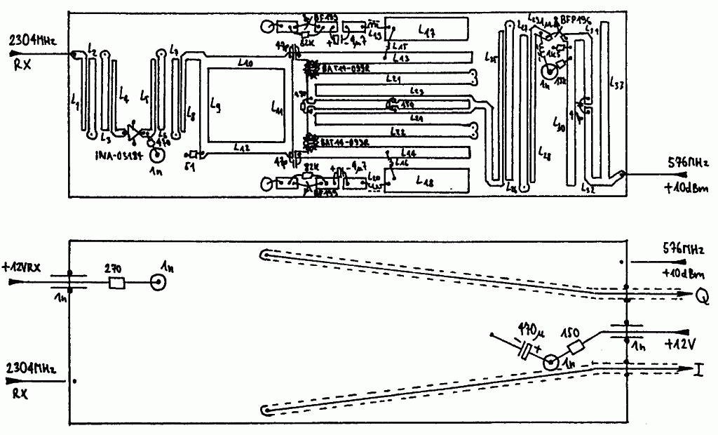
Fig.33 - 2304MHz RX mixer component location.
The circuit diagram of the quadrature receiving mixer for 5760MHz is shown on Fig.34. Since a component with the gain comparable to the INA-03184 is not available for 5.7GHz, two RF amplifier stages are required to obtain about 20dB of gain. ATF35376 HEMTs are used in both RF amplifier stages. Otherwise the circuit is almost identical to the quadrature receiving mixer for 1296MHz.
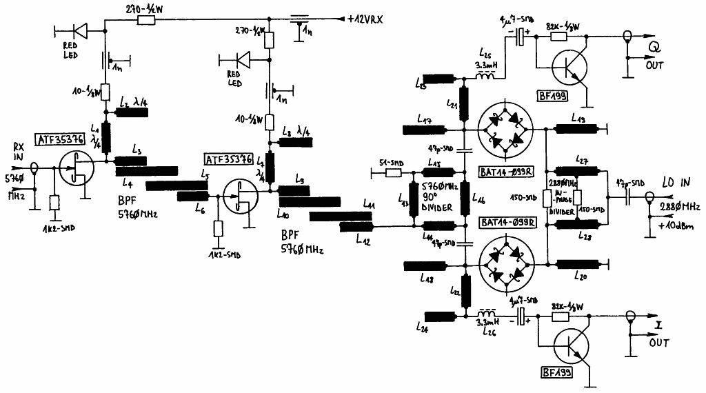
Fig.34 - Quadrature receive mixer for 5760MHz.
The quadrature receiving mixer for 5760MHz is built on a double-sided microstrip FR4 board with the dimensions of 30mmX120mm as shown on Fig.35. The corresponding component location is shown on Fig.36. The receiving mixer for 5760MHz requires no tuning.
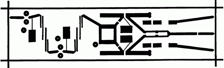
Fig.35 - 5760MHz RX mixer PCB (0.8mm double-sided FR4).
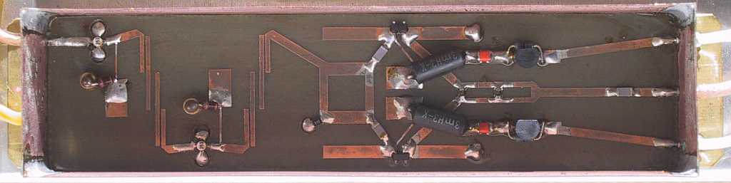

Fig.36 - 5760MHz RX mixer component location.
7. SSB zero-IF amplifier with AGC
The basic feature of direct-conversion and zero-IF receivers is to achieve most of the signal gain with simple and inexpensive AF amplifiers. Further, the selectivity is achieved with simple RC lowpass filters that require no tuning. The circuit diagram of such an IF amplifier equipped with AGC is therefore necessarily different from conventional high-IF amplifiers.
A zero-IF receiver requires a two-channel IF amplifier, since both I and Q channels need to be amplified independently before demodulation. The two IF channels should be as much identical as possible to preserve the amplitude ratio and phase offset between the I and Q signals. Therefore both channels should have a common AGC so that the amplitude ratio remains unchanged.
The circuit diagram of the quadrature SSB IF amplifier with AGC is shown on Fig.37. The IF amplifier module includes two identical lowpass filters on the input, followed by a dual-amplifier stage with a common AGC. An amplitude/phase correction is performed after the first amplifier stage, followed by another pair of lowpass filters and another
dual-amplifier stage with a common AGC.
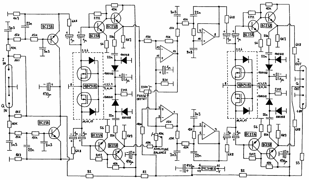
Fig.37 - Quadrature SSB IF amplifier with AGC.
The two input lowpass filters are active RC filters using BC238 emitter followers. Discrete bipolar transistors are used because much less noisy than operational amplifiers. The input circuit also provides the supply voltage to the IF preamplifiers inside the receiving mixer module through the 1.5kohm resistors.
The dual-amplifier stages are also built with discrete BC238 bipolar transistors. Each amplifier stage includes a voltage amplifier (first BC238) followed by an emitter-follower (second BC238) essentially to avoid mutual interactions when the amplifiers are chained with other circuits in the IF strip.
The AGC is using MOS transistors as variable resistors on the inputs of the dual-amplifier stages. To keep the gain of both I and Q channels identical, both MOS transistors are part of a single integrated circuit 4049UB. The digital CMOS integrated circuit 4049UB is being used in a rather uncommon way, however the remaining components inside the 4049UB act just as diodes and do not disturb the operation of the AGC.
The IF amplifier module includes two trimmers for small corrections of the amplitude balance (10kohm) and phase offset (250kohm) between the two channels. The correction stage is followed by two active RC lowpass filters using operational amplifiers (MC3403), since the signals are already large enough and the operational-amplifier noise is no longer a problem. Finally there is another, identical dual-amplifier stage with its own AGC.
The quadrature SSB IF amplifier is built on a single-sided FR4 board with the dimensions of 50mmX120mm as shown on Fig.38. The corresponding component location is shown on Fig.39. In order to keep the differences between the I and Q channels small, good quality components should be used in the IF amplifier. Using 5% resistors, 10% foil-type capacitors and conventional BC238B transistors should keep the differences between the two channels small enough for normal operation. Most components are installed vertically to save board space.
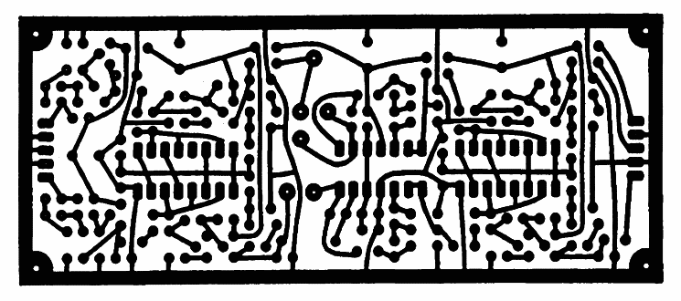
Fig.38 - IF amplifier PCB (0.8mm single-sided FR4).
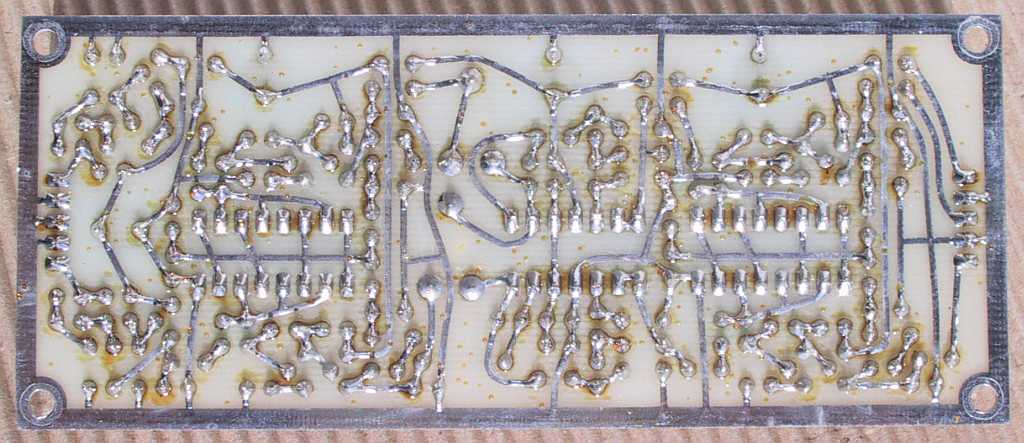
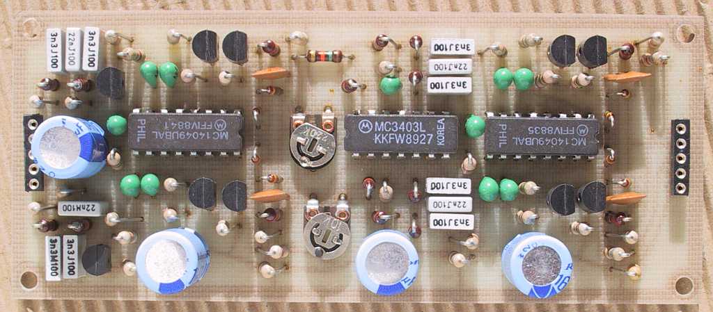
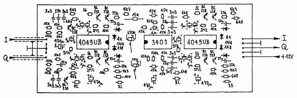
Fig.39 - IF amplifier component location.
The amplitude balance (10kohm) and phase offset (250kohm) trimmers are initially set to their neutral (central) position. These trimmers are only used while testing the complete receiver to obtain the minimum distortion of the reproduced audio signal.
8 . Quadrature SSB demodulator and AF amplifier
The main function of the quadrature SSB demodulator is the conversion of both I and Q IF signals (frequency range 0 to 1200Hz) back to the original audio frequency range from 200Hz to 2600Hz. The same module includes a power AF amplifier and a clock generator for both the phasor rotation in the transmitter and the phasor counterrotation in the receiver. The circuit diagram of the module is shown on Fig.40.
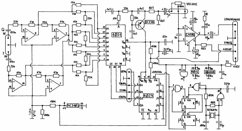
Fig.40 - Quadrature SSB demodulator and AF amplifier.
The quadrature SSB demodulator includes four operational amplifiers (MC3403) to produce an 8-phase system from the I and Q signals, using a resistor network similar to that used in the modulator. The signal demodulation or phasor counterrotation is performed by the CMOS analog switch 4051, rotating with a frequency of 1365Hz. The I and Q signals are alternatively fed to the output or in other words the circuit performs exactly the opposite operation of the modulator.
Unwanted mixing products of the phasor counterrotation are removed by an active RC lowpass (BC238). The demodulated audio signal is fed to the 100kohm volume control. A LM386 is used as the audio power amplifier due to its low current drain and small external component count.
The three clocks required to rotate both 4051 switches in the modulator and in the demodulator are supplied by a binary counter 4029. The 4029 includes an up/down input that allows the generation/demodulation of USB or LSB in this application. The up/down input has a 100kohm pullup resistor for USB operation. LSB is obtained when the up/down input is grounded through a front-panel switch.
USB/LSB switching is usually not required for terrestrial microwave work. USB/LSB switching is only required when operating through satellites or terrestrial linear transponders or when using inverting converters or transverters for other frequency bands. Finally, USB/LSB switching may be useful to attenuate interferences during CW reception. An alternative way of USB/LSB switching is interchanging the I and Q channels. When assembling together the modules of the described transceivers one should thereforecheck the wiring so that the transmitter and the receiver operate on the same sideband at the same time.
The 4029 counter requires an input clock around 11kHz. This clock does not need to be particularly stable and a RC oscillator could be sufficient. In the described transceivers a crystal source was preferred to avoid any tuning. In addition, if all transceivers use the same rotation or counterrotation frequency, the mutual interferences are reduced.
The crystal oscillator is using a clock crystal operating on a relatively low frequency of 32768Hz. The dual D-flip-flop 4013 divides this frequency by 3 to obtain a 10923Hz clock for the 4029 binary counter. The resulting rotation frequency for the 4051 switches is 1365Hz. The latter figure almost perfectly matches the hole in the frequency spectrum of human voice. The same 4029 counter also supplies the CW tone 683Hz to reduce the unwanted mixing products in the transmitter.
The quadrature SSB demodulator and AF amplifier are built on a single-sided FR4 board with the dimensions of 40mmX120mm as shown on Fig.41. The corresponding component location is shown on Fig.42. Most of the components are installed vertically to save board space.
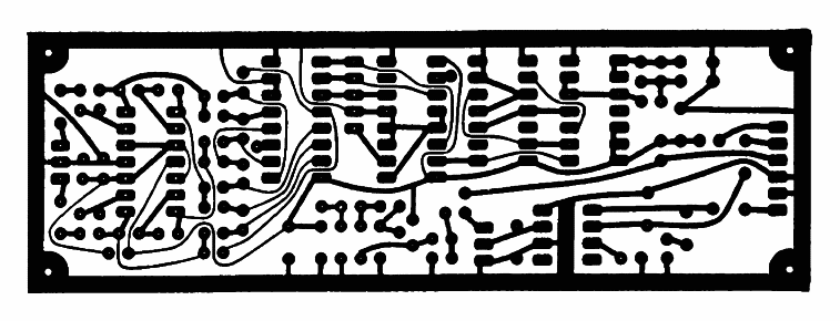
Fig.41 - Demodulator PCB (0.8mm single-sided FR4).
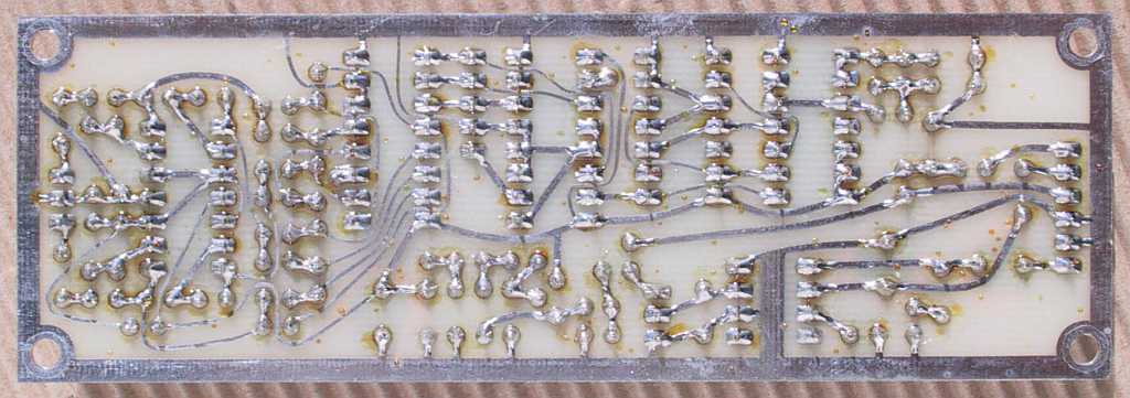
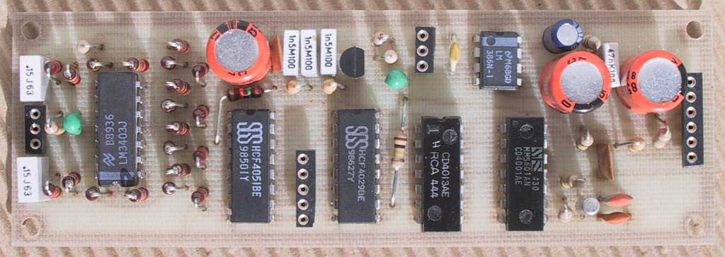
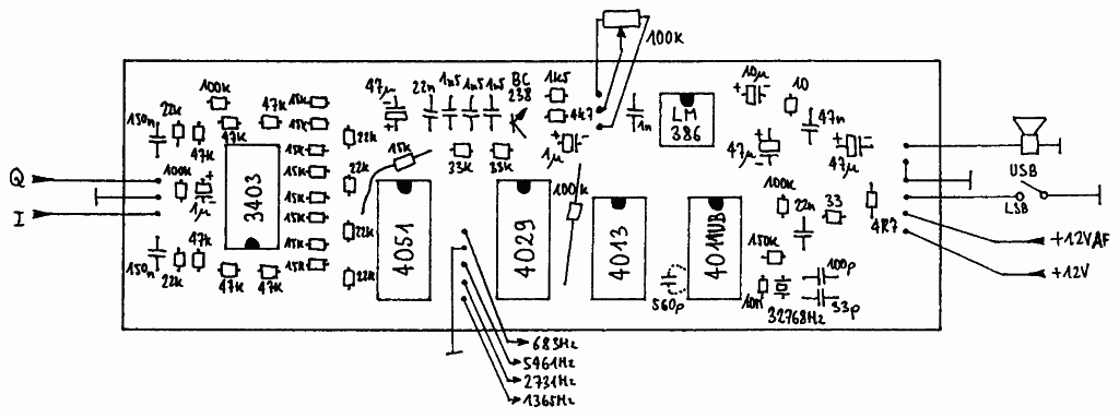
Fig.42 - Demodulator component location.
The 32768Hz crystal oscillator will only operate reliably with a 4011UB (or 4001UB) integrated circuit. The commonly available "B" series CMOS integrated circuits (4011B in this case) have a too-high gain for this application. In the latter case a 560pF capacitor may help to stabilize the oscillator. On the other hand, the oscilator circuit usually works reliably with old 4011 or 4001 circuits with an "A" suffix or no suffix letter at all.
9. SSB/CW switching RX/TX
A SSB/CW transceiver requires different switching functions. Fortunately both SSB and CW modes of operation require the same functions in the receiver. Of course two different operating modes are required for the transmitter: SSB voice and CW keying.
The RX/TX changeover is controlled by the PTT switch on the microphone in the SSB mode of operation. In the CW mode of operation, most transceivers use an automatic delay circuit to keep the transmitter enabled during CW keying. This delay circuit was perhaps required in old radios using several mechanical relays. In modern transceivers with all electronic switching it makes no sense, since the RX/TX switching can be performed in less than one millisecond.
It therefore makes sense that SSB transmission is enabled by simply pressing the PTT switch while CW transmission is enabled by pressing the CW key so that no special (and useless) controls are required on the front panel of the trasceiver. In the CW mode of operation, no delays are required and the receiver is enabled immediately after the CW key is released ("BK" mode of operation).
The circuit diagram of the SSB/CW switching RX/TX is shown on Fig.43. In the described SSB/CW transceivers, most modules are enabled at all times with a continuous +12V supply: VCXO and multipliers, receiving mixer, IF amplifier, demodulator and modulator. When enabling the transmitter either by pressing the PTT or CW keys, the RX LNA is turned off (+12VRX) and the TX PA is turned on (+12VTX and +5VTX or +4VTX).
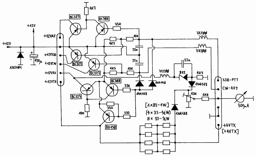
Fig.43 - SSB/CW switching RX/TX, 1296MHz (2304MHz) [5760MHz].
During SSB transmission the RX AF amplifier is turned off (+12VAF), to avoid disturbing the microphone amplifier (+12VSSB). On the other hand, during CW transmission the AF amplifier remains on as well as most receiver stages, so that CW keying can be monitored in the loudspeaker or phones. The +12VCW supply connects the 683Hz signal to the modulator input.
The supply voltages +12VAF, +12VSSB, +12VCW and +12VRX are switched by BC327 PNP transistors. Due to the higher current drain, the +12VTX supply voltage requires a more powerful PNP transistor BD138. The TX PA receives its supply voltage through a current-limiting resistor from the +12VTX line. Since the latter dissipates a considerable amount of power, it is built from several smaller resistors and located in the switching unit to prevent heating the PA transistor(s).
The value of the current-limiting resistor depends on the version of the transceiver. The 1296MHz PA with a CLY5 requires 8 pieces of 33ohm 1/2W resistors for a total value of 16.5ohms. The 2304MHz PA with a CLY2 requires 4 pieces of 33ohm 1/2W resistors for a total value of 33ohms. Finally, the 5760MHz PA with two ATF35376s requires a single 82ohm 1W resistor.
The switching module also includes the circuits to drive the front-panel meter. The latter is a moving-coil type with a full-scale sensitivity of about 300uA. The meter has two functions. During reception it is used to check the battery voltage. The 8V2 zener extends the full scale of the meter to the interesting range from about 9V to about 15V.
During transmission the meter is used to check the supply voltage of the PA transistor(s). Due to the self-biasing operation, the PA voltage will be only 0.5-1V without modulation and will rise to its full value, limited by the zener diode inside the PA, only when full drive is applied. The operation of the PA and the output RF power level can therefore be simply estimated from the PA voltage.
A S-meter is probably totally useless in small portable transceivers as those described in this article. If desired, the AGC voltge can be amplified and brought to a front-panel meter. However, one should not forget that LED indicators are not visible in full sunshine on a mountaintop, so the choice is limited to moving-coil and LCD meters.
Most components of the SSB/CW switching RX/TX are installed on a single-sided FR4 board with the dimensions of 30mmX80mm as shown on Fig.44. Their location (1296MHz version) is shown on Fig.45. Only the reverse-polarity protection diode 1N5401 and the 470uF electrolytic capacitor are installed directly on the 12V supply connector. The 10kohm trimmer is used to adjust the meter sensitivity.
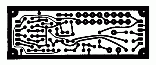
Fig.44 - SSB/CW switching RX/TX PCB (0.8mm single-sided FR4).
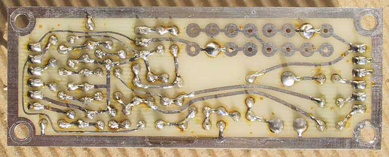
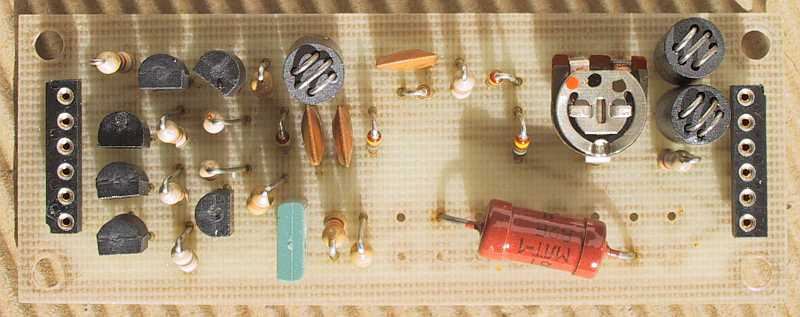
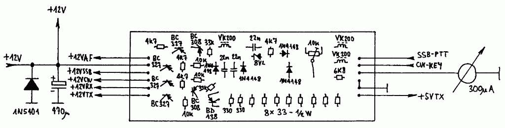
Fig.45 - SSB/CW switching RX/TX component location (1296MHz).
The 5760MHz version of the SSB/CW transceiver requires an additional PIN diode driver to provide a negative bias to the BAR80 PIN diode during reception. The corresponding circuit diagram is shown on Fig.46. The negative voltage is obtained from the 5461Hz clock, while the BC327 PNP transistor applies a positive voltage during transmission.
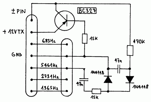
Fig.46 - PIN driver for 5760MHz.
The PIN driver is built on a small FR4 board with the dimensions of 23mmX20mm as shown on Fig.47. The corresponding component location is shown on Fig.48. The whole PIN driver module is then installed piggy-back on the demodulator board, using as support the 5-pole connector carrying the clocks to the modulator.

Fig.47 - PIN driver PCB (0.8mm single-sided FR4).
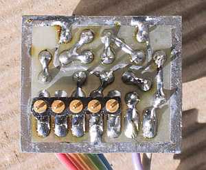
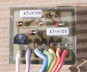
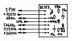
Fig.48 - PIN driver component location.
10. Construction of zero-IF SSB transceivers
The described zero-IF SSB transceivers are using many SMD parts in the RF section. SMD resistors usually do not cause any problems, since they have low parasitics up to at least 10GHz. On the other hand, there are big differences among SMD capacitors. For this reason a single value (47pF) was used anywhere. The 47pF capacitors used in the prototypes are NPO type, rather large (size 1206), have a self-resonance around 10GHz and introduce an insertion loss of about 0.5dB at 5.76GHz. Finally, the 4.7uF SMD tantalum capacitors can be replaced by the more popular tantalum "drops".
Quarter-wavelength chokes are used elsewhere in the RF circuits. In the 5760MHz transceiver all quarter-wavelength chokes are made as high-impedance microstrips. On the other hand, to save board space in the 1296MHz and 2304MHz versions, the quarter-wavelength chokes are made as small coils of 0.25mm thick copper-enameled wire of the correct length, chosen according to the frequency: 12cm for 648MHz, 9cm for 23cm mixers (648/1296MHz), 7cm for 1296MHz and for L3 on Fig.18, 5.5cm for 13cm mixers (1152/2304MHz) and 4cm for 2304MHz. The wire is tinned for about 5mm on each end and the remaining length is wound on an internal diameter of about 1mm.
The SMD semiconductor packages and pinouts are shown on Fig.49. Please note that due to lack of space, the SMD semiconductor markings are different from their type names. Only the relatively large CLY5 transistor in a SOT-223 package has enough space to carry the full marking "CLY5". The remaining components only carry one-, two- or three-letter marking codes.
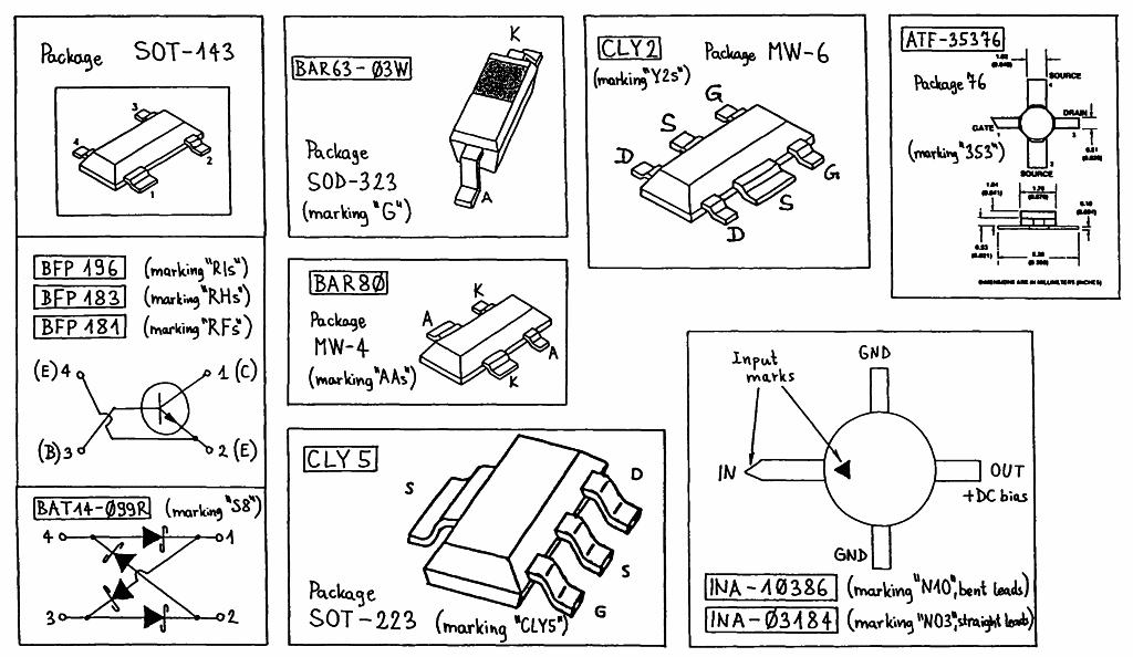
Fig.49 - SMD semiconductor packages and pinouts.
All of the microstrip circuits are built on double-sided 0.8mm thick FR4 glassfiber-epoxy laminate. Only the top side is shown in this article, since the bottom side is left unetched to act as a groundplane for the microstrips. The copper surface should not be tinned nor silver or gold plated. The copper-foil thickness should be preferably 35um.
Since the microstrip boards are not designed for plated-through holes, care should be taken to ground all components properly. Microstrip lines are grounded using 0.6mm thick silver plated wire (RG214 central conductors) inserted in 1mm diameter holes at the marked positions and soldered on both sides to the copper foil.
Resistors and semiconductors are grounded through 2mm, 3.2mm and 5mm diameter holes at the marked positions. These holes are first covered on the groundplane side with pieces of thin copper foil (0.1mm). Then the holes are filled with solder and finally the SMD component is soldered in the circuit.
Feedtrough capacitors are also installed in 3.2mm diameter holes in the microstrip boards and soldered to the groundplane. Feedthrough capacitors are used for supply voltages and low-frequency signals. Some components like bias resistors, zeners and electrolytic capacitors are installed on the bottom side (as shown on the component-location drawings) and connected to the feedthrough capacitors.
The VCXO/multiplier module and all of the microstrip circuits are installed in shielded enclosures as shown on Fig.50. Both the frame and the cover are made of 0.4mm thick brass sheet. The printed-circuit board is soldered in the frame at a height of about 10mm from the bottom. Additional feedthrough capacitors are required in the brass walls. RF signal connections are made using thin teflon-dielectric coax like RG-188. The coax braid should be well soldered to the brass frame all around the entrance hole. Finally the frame is screwed on the chassis using sheet-metal screws.
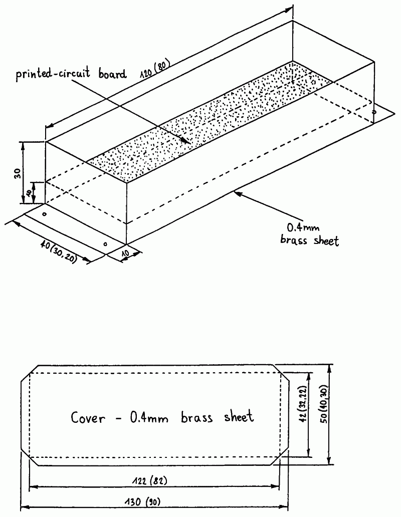
Fig.50 - Shielded RF module enclosure.
The covers are kept in place thanks to the elastic brass sheet, so they need not be soldered. An inspection of the content is therefore possible at any time. The VCXO/multiplier module is built on a single-sided board and therefore requires both a top and a bottom cover. The remaining modules are all built as microstrip circuits, so the microstrip groundplane acts as the bottom cover and only the top cover is required.
The sizes and shapes of the microstrip circuit boards are selected so that no resonances occur up to and including 2880MHz. Microwave absorber foam is therefore only required in the three modules operating at 5760MHz. To avoid disturbing the microstrip circuit, the microwave absorber foam is installed just below the top cover.
The modules of a zero-IF SSB transceiver are installed in a custom-made enclosure as shown on Fig.51. The most important component is the chassis. The latter must be made of a single piece of 1mm thick Al sheet to provide a common ground for all modules. If a common ground is not available, the receiver will probably self-oscillate in the from of "ringing" or "whistling" in the loudspeaker, especially at higher volume settings.
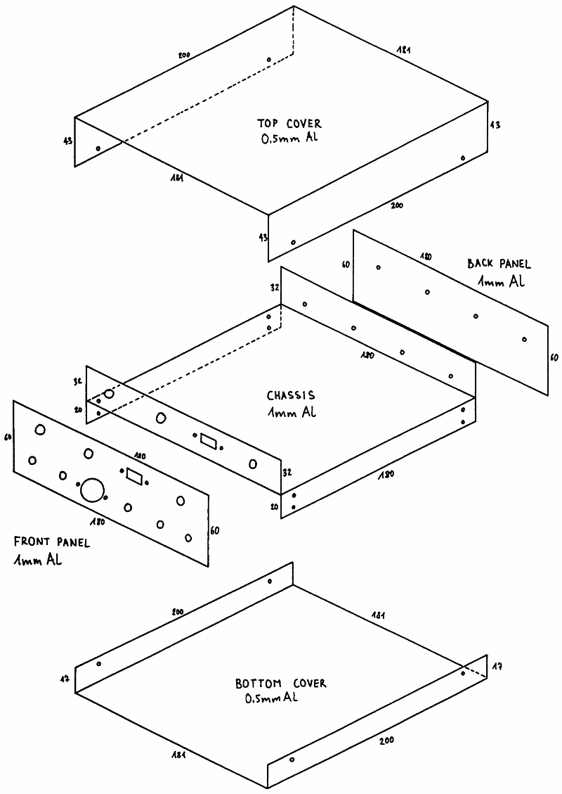
Fig.51 - Zero-IF SSB/CW transceiver enclosure.
The chassis carries both the front and back panels as well as the top and bottom covers. All of the connectors and commands are available on the front panel. The later is screwed to the chassis using the components installed: CW pushbutton, SMA connector, meter and tuning helipot. The top and bottom cover are made of 0.5mm thick Al sheet to save weight and are screwed to the chassis using sheet-metal screws.
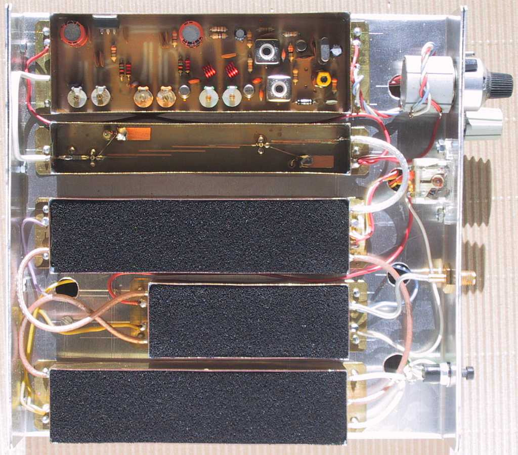
The shielded RF modules are installed on the top side of the chassis where a height up to 32mm is allowed. The audio-frequency bare printed-circuit boards are installed on the bottom side of the chassis. The interconnections between both sides of the chassis are made through five large-diameter holes.
The location of the modules of the 1296MHz or 2304MHz transceiver as well as the location of the connectors and commands on the front panel are shown on Fig.52 for both sides of the chassis. The 5760MHz transceiver has different RF modules, so the corresponding module location is shown on Fig.53. The location of the connectors and commands is the same for all three transceivers.
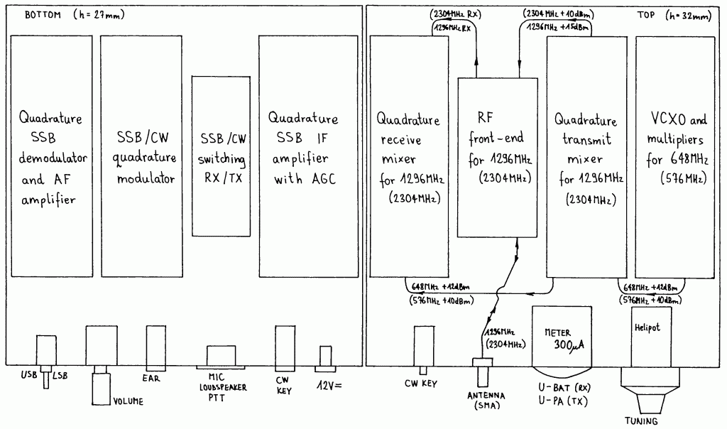
Fig.52 - 1296MHz (2304MHz) SSB/CW transceiver module location.
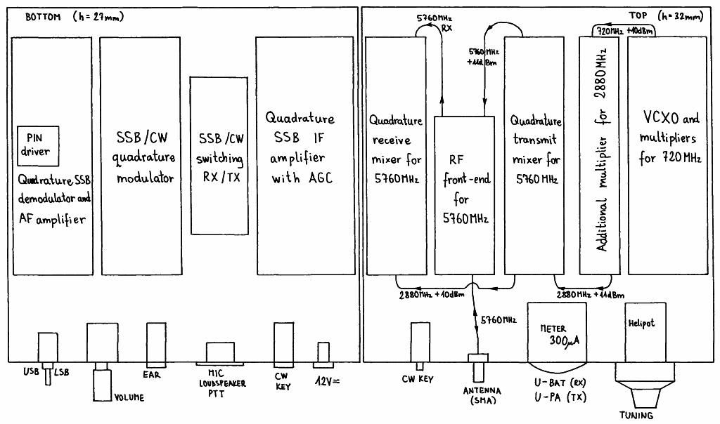
Fig.53 - 5760MHz SSB/CW transceiver module location.
The loudspeaker should not be installed inside the transceiver, since the RF receiving modules are quite sensitive to vibrations. On the other hand, the same loudspeaker may also be used as a dynamic microphone for the transmitter. The circuit is designed so that it allows a simple parallel connection of the loudspeaker output and the microphone input. The PTT and CW keys are simple switchesto ground.
12. Checkout of zero-IF SSB transceivers
The described SSB/CW transceivers for 1296MHz, 2304MHz and 5760MHz do not require much tuning. The only module that really requires tuning is the VCXO/multiplier. The latter is simply tuned for the maximum output on the desired frequency. Of course, the desired coverage of the VCXO has to be set with a frequency counter.
After the VCXO/multiplier module is adjusted, the remaining parts of the transceiver require a checkout to locate defective components, soldering errors or insufficient shielding. The receiver should already work and some noise should be heard in the loudspeaker. The noise intensity should drop when the power supply to the LNA is removed. The noise should completely disappear when the receiving mixer module is disconnected from the IF amplifier. A similar noise should be heard if only one (I or Q) IF channel is connected.
Next the receiver is connected to an outdoor antenna far away from the receiver and tuned to a weak unmodulated carrier (a beacon transmitter or another VCXO/multiplier module at a distance of a few ten meters). Tuning the receiver around the unmodulated signal one should hear both the desired tone and its much weaker mirror-image tone changing its frequency in the opposite direction. The two trimmers in the IF amplifier should be set so that the mirror tone disappears. The correct function of the USB/LSB switch can also be checked.
Finally, the shielding of the receiver should be checked. A small, handheld antenna (10-15dBi) is connected to the receiver and the main beam of the antenna is directed into the transceiver. If the noise coming from the loudspeaker changes, the shielding of the local oscillator multiplier chain is insufficient.
Next a mains-operated fluorescent tube (20W or 40W) is turned on in the same room. A weak mains hum should only be heard when the handheld antenna is pointed towards the tube at 2-3m distance. If a clean hum without noise is heard regardless of the antenna direction, the shielding of the local-oscillator multiplier chain is insufficient.
The transmitter should be essentially checked for the output power. The full output power should be achieved with the trimmer in the modulator in a middle position in CW mode. The DC voltage across the PA transistor should rise to the full value allowed by the 5.6V or 4.7V zener diode. The output power should drop by an equal amount if only
I or only Q modulation is connected to the transmit mixer.
Finally the SSB modulation has to be checked with another receiver for the same frequency band or best in a contact with another amateur station at a distance of a few km. This is the simplest way to find out the correct sideband, USB or LSB, of the transmitter, since the I and Q channels can be easily interchanged by mistake in the wiring.
The residual carrier level of the transmit mixer should also be checked. Due to the conversion principle this carrier results in a 1365Hz tone in a correctly-tuned SSB receiver. The carrier suppression may range from -35dB in the 1296MHz RTX down to only -20dB in the 5760MHz RTX. A poor carrier suppression may be caused by a too high LO signal level or by a careless installation of the BAT14-099R mixer diodes. Note that the residual carrier can not be monitored on another correctly-tuned zero-IF receiver, since it falls in the AF response hole of the zero-IF receiver.
The current drain of the described transceivers should be as follows. Receivers: 1296MHz:105mA, 2304MHz:175mA and 5760MHz:300mA. The current drain of the transmitters is inversely proportional to the output power due to the self-biasing of the PA. The minimum current drain corresponds to SSB modulation peaks or CW transmission. Transmitters: 1296MHz:650-870mA, 2304MHz:490-640mA and 5760MHz:410-440mA. All figures are given for a typical sample at a supply voltage of 12.6V.
At the end, one should understand that zero-IF transceivers also have some limitations. In particular, the dynamic range of the receiver is limited by the direct AM detection in the receiving mixer. If very strong signals are expected, the LNA gain has to be reduced to avoid the above problem. This is already done in the 1296MHz receiver, since strong radar signals are quite common in the 23cm band. The sensitivity to radar interference of the described zero-IF 1296MHz transceiver was found comparable to the conventional transverter + 2mRTX combination.
On the other hand, the 2304MHz and 5760MHz transceivers have a higher gain LNA. If the dynamic range needs to be improved, the second LNA stage can simply be replaced with a wire bridge in both transceivers. Of course, the internal LNA gain has to be reduced or the LNA has to be completely eliminated if an external LNA is used.
* * * * *