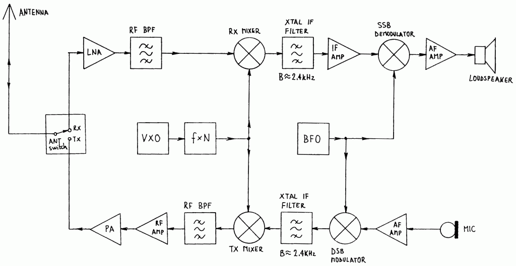
Fig.1 - Conventional (high-IF) SSB transceiver design.
(ZIF SSB)
(1.3, 2.3 & 5.7GHz)
(10GHz)
(3.4GHz)
(24GHz)
(HOME)
NO-TUNE ZERO-IF MICROWAVE SSB/CW TRANSCEIVERS
Matjaz Vidmar, S53MV
1. Microwave SSB transceiver design
When discussing SSB transceivers, the first question to be answered is probably the following: does it make sense to develop and build new SSB radios? Today SSB transceivers are mass-produced items for frequencies below 30MHz. There is much less choice on the market for 144MHz or 432MHz SSB transceivers and there are just a few products available for 1296MHz or even higher frequencies.
Most radio-amateurs are therefore using a base SSB transceiver (usually a commercial product) operating on a lower frequency and suitable receive and transmit converters or transverters to operate on 1296MHz or higher frequencies. The most popular base transceiver is certainly the good old IC202. All narrow-band (SSB/CW) microwave activity is therefore concentrated in the first 200kHz of amateur microwave segments like 1296.000-1296.200, 2304.000-2304.200 etc due to the limited frequency coverage of the IC202.
Transverters should always be considered a poor technical solution for many reasons. Receive converters usually degrade the dynamic range of the receiver while transmit converters dissipate most of the RF power generated in the base SSB transceiver. Both receive and transmit converters generate a number of spurious mixing products that are very difficult to filter out due to the harmonic relationships among the amateur frequency bands 144/432/1296...
However, the worst problem of most transverters is the breakthrough of strong signals in or out of the base-transceiver intermediate-frequency band. This problem seems to be worst when using a 144MHz first IF. Strong 144MHz stations with big antenna arrays may break in the first IF even at distances of 50 or 100km. Since the problem is reciprocal, a careless microwave operator may even establish two-way contacts on 144MHz although using a transverter and antenna for 1296MHz or higher frequencies.
Some microwave operators solved the above problem by installing a different crystal in the transverter, so that for example 1296.000MHz is converted to a less used segment around 144.700MHz. Serious microwave contestmen use transverters with a first IF of 28MHz, 50MHz or even 70MHz to avoid the abovementioned problem. Neither solution is cheap. The biggest problem is to carry a large 144MHz or HF all-mode transceiver together with a suitable power supply on a mountaintop.
Even the good old IC202 has its own problems. This radio is no longer being manufactured for more than a decade. New radios can not be purchased while the maintenance of the old ones is becoming difficult. Second-hand radios are usually found in very poor conditions due to the many "modifications" and "improvements" made by their previous owners.
As a conclusion, today it still makes sense to develop and build SSB radios for 1296MHz and higher frequencies. Since the abovementioned problems of the transverters are well known and are not really new, many technical solutions were considered by different designers. Most solutions were discarded simply because too complex, too expensive and too difficult to build, even when compared to the already complex combination of a base RTX and transverter.
Most commercial SSB transceivers include a modulator and a demodulator operating on a high IF, as shown on Fig.1. The resulting SSB signal is converted to the RF operating frequency in the transmitter and back to the IF in the receiver. Both the transmitter and the receiver use expensive components like crystal filters. Besides crystal filters, additional filtering is required in the RF section to attenuate image responses and spurious products of both receiving and transmitting mixers.
Fig.1 - Conventional (high-IF) SSB transceiver design.
The design of conventional (high-IF) SSB transceivers dates back to the vacuum-tube age, when active components (tubes) were expensive and unreliable. Passive components like filters were not so critical. Complicated tuning procedures only represented a small fraction of the overall cost of a vacuum-tube SSB transceiver.
SSB crystal filters usually operate in the frequency range around 10MHz. A double or even triple upconversion is required to reach microwave frequencies in the transmitter. On the other hand, a double or triple downconversion is required in the receiver to get back to the crystal-filter frequency. Commercial VHF/UHF SSB transceivers therefore save some expensive components by sharing some stages between the transmitter and the receiver.
A conventional microwave SSB transceiver is therefore complicated and expensive. Building such a transceiver in amateur conditions is difficult at best. Lots of work as well as some microwave test equipment is required. The final result is certainly not cheaper and may not perform better than the well-known transverter + base RTX combination.
Fortunately, expensive crystal filters and complicated conversions are not essential components of a SSB transceiver. There are other SSB transceiver designs that are both cheaper and easier to build in amateur conditions. The most popular seems to be the direct-conversion SSB transceiver design shown on Fig.2. A direct-conversion SSB receiver achieves most of its gain in a simple audio-frequency amplifier, while the selectivity is achieved by simple RC lowpass filters.
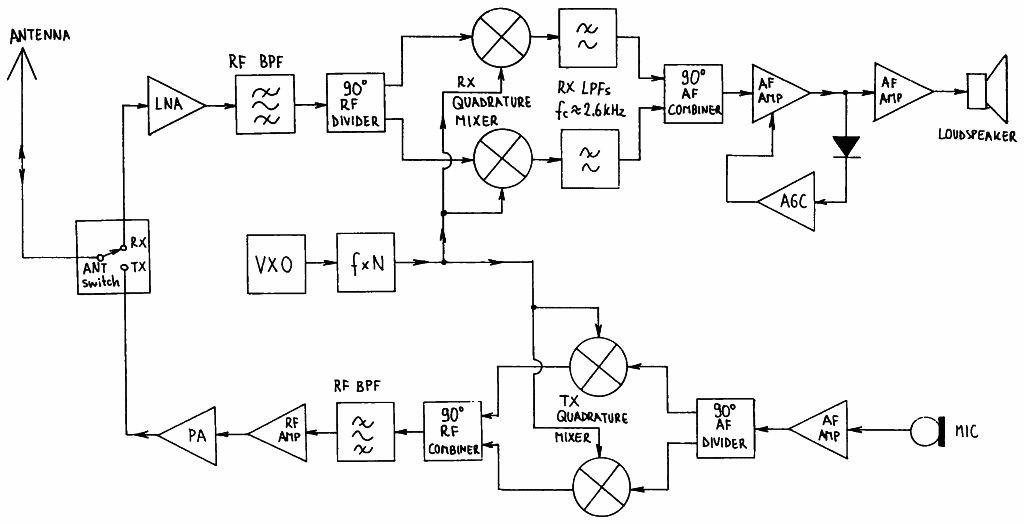
Fig.2 - Direct-conversion SSB transceiver design.
The most important feature of a direct-conversion SSB transceiver is that there are no complicated conversions nor image frequencies to be filtered out. The RF section of a direct-conversion SSB transceiver only requires simple LC filters to attenuate far-away spurious responses like harmonics and subharmonics. In a well designed direct-conversion SSB transceiver, the RF section may not require any tuning at all.
The most important drawback of a direct-conversion SSB transceiver is a rather poor unwanted sideband rejection. The transmitter includes two identical mixers operating at 90 degrees phase shift (quadrature mixer) to obtain only one sideband. The receiver also includes two identical mixers operating at 90 degrees phase shift to receive just one sideband and suppress the other sideband. A direct-conversion SSB transceiver operates correctly only if the gain of both mixers is the same and the phase shift is exactly 90 degrees.
A direct-conversion SSB transceiver therefore includes some critical components like precision (1%) resistors, precision (2%) capacitors, selected or "paired" semiconductors in the mixers and complicated phase-shifting networks. The most complicated part is usually the audio-frequency 90-degree divider or combiner including several operational amplifiers, precision resistors and capacitors. Although using precision components, the unwanted sideband rejection will seldom be better than -40dB. This is certainly not enough for serious work on HF.
In spite of the abovementioned difficulties, direct-conversion designs are quite popular among the builders of QRP HF transceivers. At frequencies above 30MHz it is increasingly more difficult to obtain accurate phase shifts. Due to the low natural (antenna) noise above 30MHz, a low-noise RF amplifier is usually used to improve the mixer noise figure. A LNA may cause direct AM detection in the mixers. A LNA may also corrupt the amplitude balance and phase offset of the two mixers, if the local oscillator signal is picked up by the antenna. A VHF direct-conversion SSB transceiver is therefore not as simple as its HF counterpart.
On the other hand, a direct-conversion SSB design has important advantages over conventional SSB transceivers with crystal filters, since there are no image frequencies and less spurious responses. Professional (military) SSB transceivers therefore use direct conversion, but the AF phase shifts are obtained by digital signal processing. The DSP uses an adaptive algorithm to measure and compensate any errors like amplitude unbalance or phase offset of the two mixers, to obtain a perfect unwanted sideband rejection.
Additional AF signal processing also allows a different SSB transceiver design, for example a SSB transceiver with a zero IF as shown on Fig.3. The latter is very similar to a direct-conversion RTX except that the local oscillator is operating in the center of the SSB signal spectrum, in other words at an offset of about 1.4kHz with respect to the SSB suppressed carrier frequency.
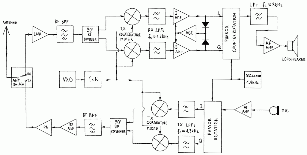
Fig.3 - Zero-IF SSB transceiver design.
In a zero-IF SSB transceiver (also called "Weaver" SSB transceiver or just receiver), the audio frequency band from 200Hz to 2600Hz is converted in two bands from 0 to 1200Hz. Lowpass filters therefore have a cutoff frequency of 1200Hz, thus allowing a high rejection of the unwanted sideband. A zero-IF SSB transceiver therefore retains all of the advantages of a direct-conversion design and solves the problem of the unwanted-sideband rejection.
The quadrature IF amplifier of a zero-IF SSB transceiver includes two conventional AF amplifiers. Since the latter are usually AC coupled, the missing DC component will be converted in the demodulator in a hole in the AF response around 1.4kHz. Fortunately this hole is not harmful at all for voice communications, since it coincides with a hole in the spectrum of the human voice. In fact, some voice-communication equipment includes notch filters to create an artificial hole around 1.4kHz to improve the signal-to-noise ratio and/or to add a low-baud-rate-telemetry channel to the voice channel. Therefore a potential drawback of a zero-IF design is actually an advantage for voice communications.
Like a direct-conversion RTX, a zero-IF SSB transceiver also requires quadrature transmit and receive mixers. However, amplitude unbalance or phase errors are much less critical, since they only cause distortion of the recovered audio signal. Conventional components, like 5% resistors, 10% capacitors and unselected semiconductors may be used anywhere in a zero-IF SSB transceiver.
Finally, a zero-IF SSB transceiver does not require complicated phase-shifting networks. Both the quadrature modulator in the transmitter and the quadrature demodulator in the receiver (phasor rotation and counterrotation with 1.4kHz) are made by simple rotating switches and fixed resistor/opamp networks. CMOS analog switches like the 4051 are ideal for this purpose, rotated by digital signals coming from a 1.4kHz oscillator.
Although the block diagram of a zero-IF SSB transceiver looks complicated, such a transceiver is relatively easy to build. In particular, very little (if any) tuning is required, since there are no critical components used anywhere in the transceiver. In particular, the RF section only includes relatively wideband (10%) bandpass filters that require no tuning. The IF/AF section also accepts wide component tolerances and thus requires no tuning. The only remaining circuit is the RF local oscillator. The latter may need some tuning to bring the radio to the desired operating frequency...
The described zero-IF concept should allow the design of simple and efficient SSB transceivers for an arbitrary frequency band. Three successful designs of zero-IF SSB transceivers covering the lower amateur microwave bands of 1296MHz, 2304MHz and 5760MHz will be briefly described in this article. Similar technical solutions were first tested in PSK packet-radio transceivers operating at 1.2Mbit/s in the 23cm and 13cm amateur frequency bands.
2. Microwave SSB transceiver technology
Of course several requirements and technology issues need to be considered before a theoretical concept can materialize in a real-world transceiver. Fortunately the requirements are not severe for the lower amateur microwave bands. In this frequency range no very strong signals are expected, so there are no special requirements on the dynamic range of the receiver. Only a relatively limited frequency range needs to be covered (200 to 400kHz in each band) and this can be easily achieved using a VXO and multipliers as the local oscillator.
From the technology point of view it is certainly convenient to use up-to-date components. High-performance and inexpensive microwave semiconductors were developed first for satellite-TV receivers and then for mobile communications like GSM or DECT telephones. These new devices provide up to 25dB of gain per stage up to 2.3GHz and up to 14dB of gain per stage up to 10GHz. Many other functions, like schottky mixer diodes or antenna-switching PIN diodes are also available.
Using obsolete components makes designs complicated. For example, the well known transistors BFR34A and BFR91 were introduced almost 25 years ago. At that time they were great devices providing almost 5dB of gain at 2.3GHz. Today it makes more sense to use an INA-03184 MMIC to get 25dB of gain at 2.3GHz or in other words replace a chain of 5 (five) amplifier stages with the abovementioned obsolete transistors.
The availability of active components also influences the selection of passive components. Many years ago, all microwave circuits were built in waveguide technology. Waveguides allow very low circuit losses and high-Q resonators. Semiconductor microwave devices introduced microstrip circuits built on low-loss substrates like alumina (Al2O3) ceramic or glassfiber-teflon laminates. Conventional glassfiber-epoxy laminates like FR4 were not used above 2GHz due to the high losses and poor Q of microstrip resonators.
However, a zero-IF SSB transceiver design does not require a very high selectivity in the RF section. If the circuit losses can be compensated by high-gain semiconductor devices, cheaper substrates like the conventional glassfiber-epoxy FR4 can be used at frequencies up to at least 10GHz. The FR4 laminate has excellent mechanical properties. Unlike soft teflon laminates, cutting, drilling and hole plating in FR4 is well known. Even more important, most SMD component packages are designed for installation on a FR4 substrate and may break or develop intermittent contacts if installed on a soft teflon board.
Therefore, losses in FR4 microstrip transmission lines and filters were investigated. Surprisingly, the losses were found inversely proportional to board thickness and rather slowly increasing with frequency. This simply means that the FR4 RF losses are mainly copper losses, while dielectric losses are still rather low. FR4 RF copper losses are high since the copper surface is made very rough to ensure good mechanical bonding to the dielectric substrate.
In fact, if the copper foil is peeled off a piece of FR4 laminate, the lower foil surface is rather dark. On the other hand, if the copper foil is peeled off a piece of microwave teflon laminate, the colors of both foil surfaces are similar. Since different manufacturers use different methods for bonding the copper foil, RF losses are different in different FR4 laminates. On the other hand, the dielectric constant of FR4 was found quite stable. Finally, silver or gold plating of microstrip lines etched on FR4 laminate really makes no sense, since most of the RF losses are caused by the (inaccessible) rough foil surface bonded to the dielectric.
A practical FR4 laminate thickness for microwave circuits with SMD components is probably 0.8mm. A 50-ohm microstrip line has a width of about 1.5mm and about 0.2dB/cm of loss at 5.76GHz. Therefore microstrip lines have to be kept short if etched on FR4 laminate. For comparison, the FR4 microstrip losses are about three times larger than the microstrip losses of a glassfiber-teflon board and about ten times larger than the losses of teflon semirigid coax cables.
Although FR4 laminate losses are high, resonators and filters can still be implemented as microstrip circuits. Considering PCB etching tolerances and especially underetching, both transmission lines and gaps in between them should not be made to narrow. A practical lower limit is 0.4mm width for the transmission lines and 0.3mm for the gaps.
A practical 5.76GHz two-resonator bandpass design is shown on Fig.4. The measured insertion loss of 3.5dB is referred to the worst-case, very lossy FR4. A better FR4 could get down to 3dB or even 2.5dB. Although an insertion loss of 3.5dB is rather high for a 10% bandwidth filter, it can easily be recovered with modern high-gain semiconductor devices. For comparison, the insertion loss of a SMD coupling capacitor may be as high as 0.5dB.
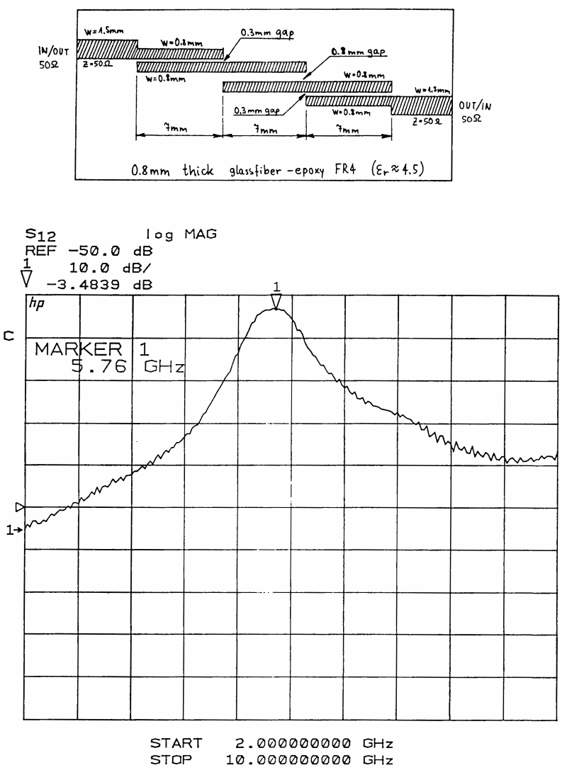
Fig.4 - 5.76GHz bandpass filter response.
As already mentioned, modern semiconductor devices are really easy to use even at microwave frequencies. Silicon MMIC amplifiers provide 25dB of gain (limited by package parasitics) up to 2.3GHz. If less gain is required, conventional silicon bipolar transistors can be used, since their input and output impedances are also close to 50ohms.
GaAs semiconductors are more practical above about 5GHz. In particular, high performance devices like HEMTs became inexpensive since they are mass produced for satellite-TV receivers. HEMTs operate at lower voltages and higher currents than conventional GaAsFETs, so their input and output impedances are very close to 50ohms at frequencies above 5GHz.
Serious microwave engineers are afraid of using HEMTs since these devices have enough gain to oscillate at frequencies above 50GHz or even 100GHz. In this case it is actually an advantage to build the circuit on a lossy laminate like FR4, since the latter will efficiently suppress any oscillations in the millimeter frequency range. Having the ability to control the loss in a circuit therefore may represent an advantage!
The availability of inexpensive power GaAsFETs greatly simplifies the construction of transmitter output stages. In particular, the high gain of power GaAsFETs in the 23cm and 13cm bands greatly reduces the number of stages when compared to silicon bipolar solutions.
Zero-IF and direct-conversion transceivers have some additional requirements for mixers. Mixer balancing is very important, both to suppress the unwanted residual carrier in the transmitter and to suppress the unwanted AM detection in the receiver. At microwave frequencies, the simplest way of achieving good mixer balancing is to use a subharmonic mixer with two antiparallel diodes as shown on Fig.5.
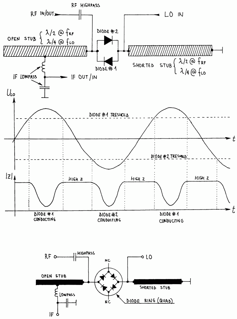
Fig.5 - Subharmonic mixer design.
Such a mixer requires a local oscillator at half frequency. Frequency doubling is achieved internally in the mixer circuit. A disadvantage of this mixer is a higher noise figure in the range 10 to 15dB and sensitivity to the LO signal level. Both a too-low LO drive or a too-high LO drive will further increase the mixer insertion loss and noise
figure.
On the other hand, the abovementioned subharmonic mixer only requires two non-critical microstrip resonators that do not influence the balancing of the mixer. The best performances were obtained using schottky quads with the four diodes internally connected in a ring. The schottky quad BAT14-099R provides about -35dB of carrier suppression at 1296MHz and about -25dB of carrier suppression at 5760MHz with no tuning.
A very important advantage of the subharmonic mixer is that the local oscillator operates at half of the RF frequency. This reduces the RF-LO crosstalk and therefore the shielding requirements in zero-IF or direct-conversion transceivers. A side advantage is that the half-frequency LO chain requires less multiplier stages.
The IF/AF signal processing includes a quadrature modulator in the transmitter and a quadrature demodulator in the receiver. Although the abovementioned functions look complicated in the block diagram, they translate in a relatively simple practical circuit diagram. Both the modulator and demodulator require two balanced mixers operating at a 90-degree phase shift in the audio frequency range. The same function can also be described (and implemented!) as phasor rotation or counterrotation.
Phasor rotation can simply be achieved in a multiphase system using a rotating switch to select the desired phase. The larger the number of available phases, the better the resolution of the phasor rotation. The absolute minimum is four different phases. In a SSB demodulator, filtering is much simplified if at least 8 phases are used. Finally, a BPSK demodulator requires an even better resolution and 16 phases are recommended.
A quadrature IF chain has two channels: I and Q. A four-phase system can easily be obtained by adding the inverted I and Q signals. In fact, a system with an arbitrary number of phases can be generated from linear combinations of the I and Q signals. In other words, if four phases: I, Q and their inverted replicas are available, any number of phases can be generated by simple resistor networks.
The above theory is easily explained on the circuit diagram of the SSB quadrature demodulator shown on Fig.6. The four signals I, Q and their inverted replicas drive a resistor network (8 resistors R1=15kohm and 4 resistors R2=22kohm) to generate an 8-phase system. The output signal is taken from a rotating switch. The direction of the switch rotation determines whether USB (counter-clockwise) or LSB (clockwise) is demodulated.
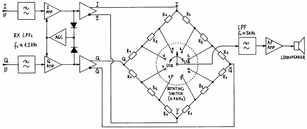
Fig.6 - SSB quadrature demodulator.
There are no particular requirements for the switch, so a conventional 4051 CMOS 1-of-8 analog switch can be used, together with standard 5% resistors R1 and R2. The switch is rotated by an up/down counter and clock generator, built with compatible 40xx CMOS logic devices. Of course, since a finite number of phases is used, a 3kHz lowpass is required to remove the phase quantization steps and switching transients before the audio amplifier.
The SSB quadrature modulator should perform exactly the opposite operation, so similar hardware can be used. However, in the modulator the rotating switch is used to distribute the input AF signal to the I and Q outputs as shown on Fig.7. The R1/R2 resistor network drives "virtual-ground" inputs provided by operational amplifiers. After phasor rotation, the unwanted mixing products must be removed by two 1.2kHz lowpass filters.
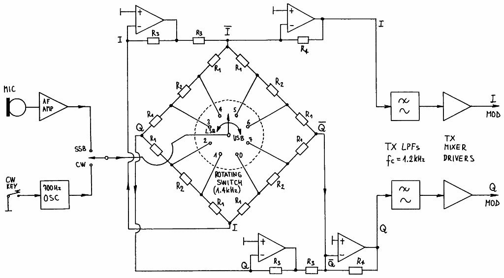
Fig.7 - SSB/CW quadrature modulator.
Finally, the described quadrature modulator can also be used to generate a CW signal by providing a 700Hz sinewave on the input. Of course this method does not generate a particularly clean output carrier. The number and magnitude of spurious outputs can be reduced if the 700Hz sinewave is derived by dividing by two the 1.4kHz switch rotation frequency.
3. Practical implementation of microwave SSB transceivers
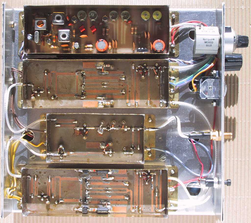
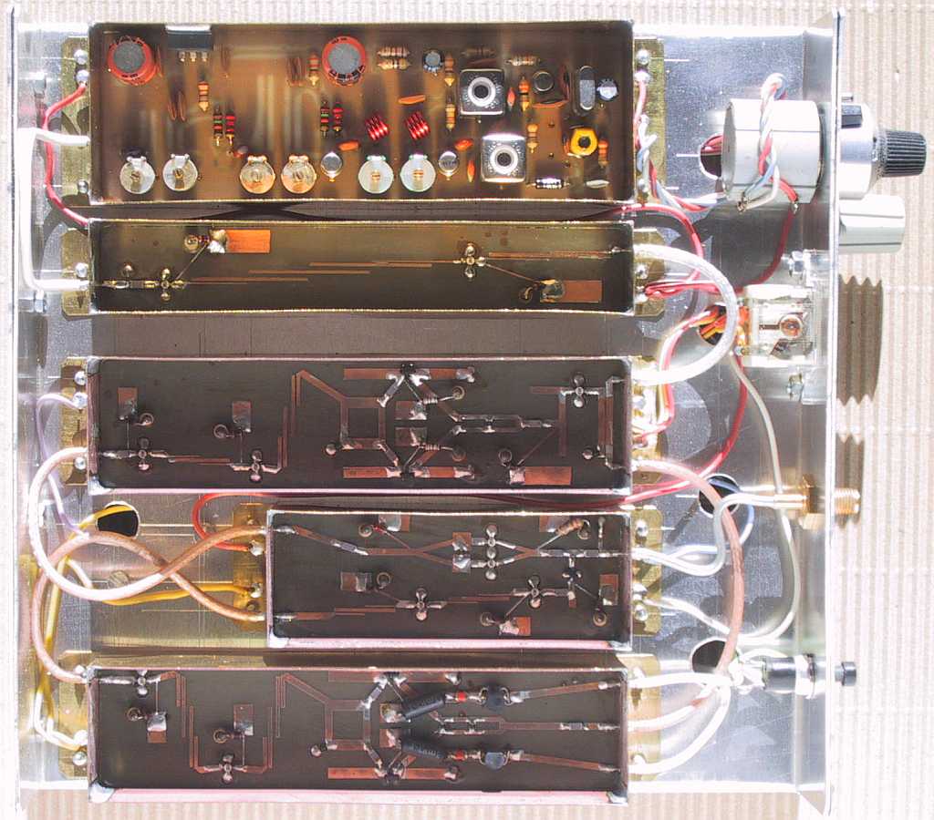
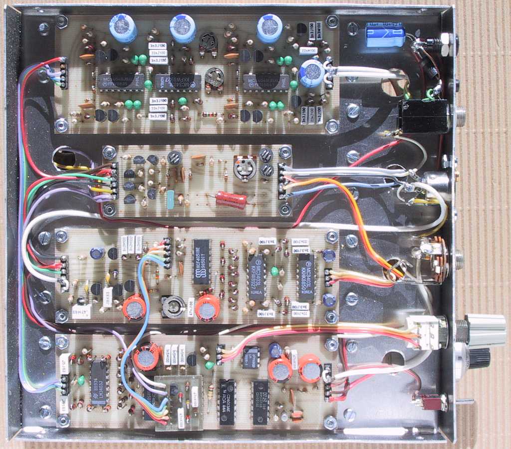
The three zero-IF SSB transceivers for 1296MHz, 2304MHz and 5760MHz have many parts in common. In particular, the AF and IF sections are identical in all three transceivers. The RF sections are similar, however the microstrip filters are necessarily different as well as the low-noise and power devices used in each frequency band. Finally, the same VCXO module is used, with small modifications, in all three transceivers.
The block diagram of the RF section of the 1296MHz transceiver is shown on Fig.8. A VCXO is used to cover about 250kHz (23cm narrowband SSB/CW segment). The VCXO is followed by a conventional chain of frequency multiplers with silicon bipolar transistors, built on a conventional single-sided printed-circuit board. A 10-turn helipot is used for tuning resulting in a tuning rate of 25kHz per turn or 500Hz per division on the tuning dial.

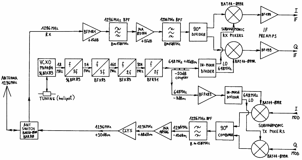
Fig.8 - Block diagram of the RF section for 1296MHz.
The remaining circuits of the 23cm SSB transceiver are built on three microstrip circuit boards etched on 0.8mm thick, double-sided FR4 laminate. The three RF modules include the transmitting mixer, the RF front-end ant the receiving mixer. The TX mixer module includes a -20dB LO coupler and amplifier (BFP183), two subharmonic mixers (two BAT14-099R) operating in quadrature and the RF driver amplifier INA10386.
The RF front-end module includes the TX power amplifier (CLY5), the antenna switch with PIN diodes BAR63-03W and BAR80 and the RX LNA (BFP181). Finally, the RX mixer module includes further RF gain (INA03184), two subharmonic mixers (two BAT14-099R) operating in quadrature and two IF preamplifiers (two BF199).
Since the zero-IF SSB transceiver concept does not require high-selectivity RF filters, all filters are built as simple microstrip circuits with quarter-wavelength resonators with the bandwidth exceeding 10% of the central frequency. Due to the relatively low Q and wide bandwidth, the laminate and etching tolerances are close enough so that no additional tuning of the microstrip resonators is required.
Since interference from powerful non-amateur transmitters (radars and other pulse transmissions) is rather common in the 23cm band, the gain of the RX LNA has to be kept as low as possible to prevent direct detection in the receiving mixers. On the other hand, higher-gain LNAs, optimized for noise figure, can be used in the 13cm and 5cm bands.
The block diagram of the RF section of the 2304(2320)MHz transceiver is shown on Fig.9. Although the relative VCXO coverage is reduced when compared to the 1296MHz version, the absolute coverage is extended to cover a 300kHz wide segment due to the higher frequency-multiplication factor. A coverage of 300kHz should be enough for narrowband (SSB/CW) operation and allow for some crystal-frequency drift at the same time.
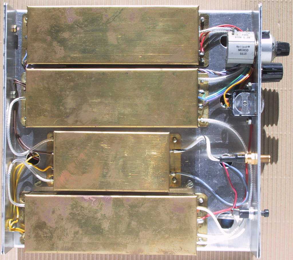
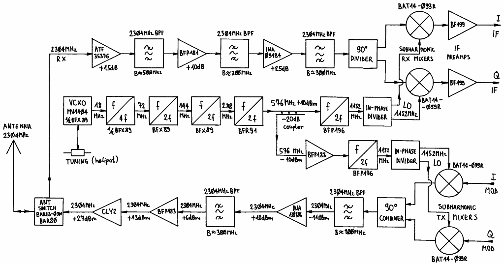
Fig.9 - Block diagram of the RF section for 2304MHz.
In the 13cm SSB transceiver the VCXO module only provides a frequency of 576MHz. The last multiplier stages are included in the transmitter and receiver mixer modules, since they are built as microstrip circuits. The TX mixer module therefore includes a -20dB LO coupler and amplifier (BFP183), an 1152MHz frequency doubler (BFP196), two subharmonic mixers (two BAT14-099R) operating in quadrature and the first RF amplifier INA10386.
Since the gain of silicon transistors becomes rather low above 4GHz, the whole RF section of the 5cm SSB transceiver is designed with HEMTs (ATF35376). These devices are no longer expensive and are easily available, since they are manufactured in large quantities to be used in 12GHz satellite-TV LNAs and LNCs. Unfortunately there are no inexpensive power devices available for the 5.76GHz band yet (like the CLY... series for frequencies below 3GHz), so the 5cm TX provides only 100mW with two low-power HEMTs ATF35376 in parallel.
The operation of the quadrature modulator and demodulator has already been discussed in detail. Both are driven by a common clock generator synchronized to a 32.768kHz crystal. The resulting rotation/counterrotation frequency is 1365Hz. The 4051 rotating switches receive 5641Hz, 2731Hz and 1365Hz clocks, while the resulting CW tone frequency is 683Hz.
* * * * *
The RF front-end includes a two-stage (BFP183 and CLY2) TX power amplifier, a PIN-diode antenna switch (BAR63-03W and BAR80) and a two-stage RX LNA (ATF35376 and BFP181). A third RX RF amplifier stage (INA03184) is included in the receive mixer module together with two subharmonic mixers (two BAT14-099R) operating in quadrature, two IF preamplifiers (two BF199) and a separate LO doubler stage to 1152MHz (BFP196).
The block diagram of the RF section of the 5760MHz transceiver is shown on Fig.10. Due to the higher operating frequency, the multiplier chain following the VCXO requires even more stages. Therefore the VCXO itself and the multipliers up to 720MHz are built on a single-sided board, while the final multiplier to 2880MHz and amplifier are built as a microstrip circuit. The VCXO covers a frequency band of about 400kHz around 5.76GHz to allow for some crystal-frequency drift.

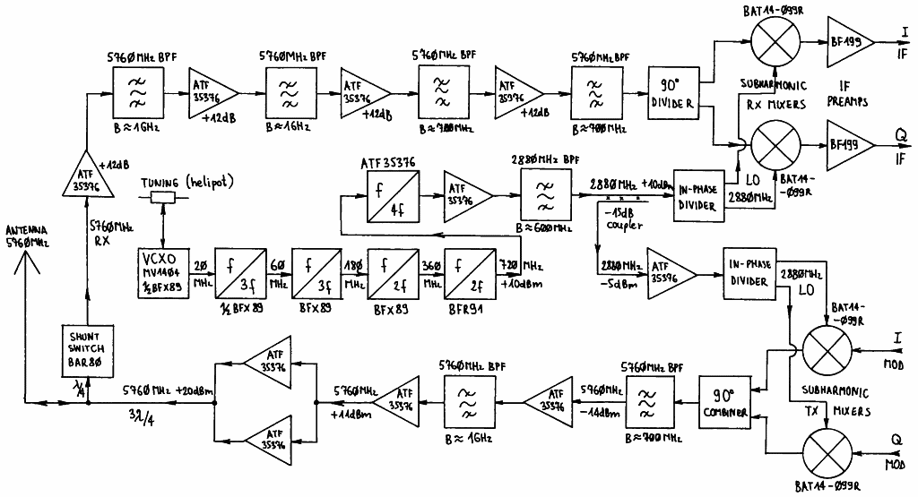
Fig.10 - Block diagram of the RF section for 5760MHz.
The 5cm TX mixer modules includes similar stages to the 23cm TX mixer: a -15dB LO coupler and 2880MHz amplifier (ATF35376), two subharmonic mixers (two BAT14-099R) and two RF amplifier stages (two ATF35376) to raise the signal level to about 12mW. The TX power amplifier is located in the RF front-end module together with a two stage LNA (two ATF35376) and the antenna switch (BAR80). Finally, the RX mixer module includes two additional RF amplifier stages, two subharmonic mixers (BAT14-099R) and two IF preamplifiers (two BF199).
The 5.76GHz microstrip circuits are also etched on double-sided FR4 laminate. Most of the bandpass filters are built as half-wave resonators open at both ends to avoid RF grounding problems. The antenna switch includes a single shunt diode BAR80, since series PIN diodes are useless above 5GHz. The transmitter power amplifier is therefore specially biased during reception so that its output impedance is transformed into an open circuit for the receiver.
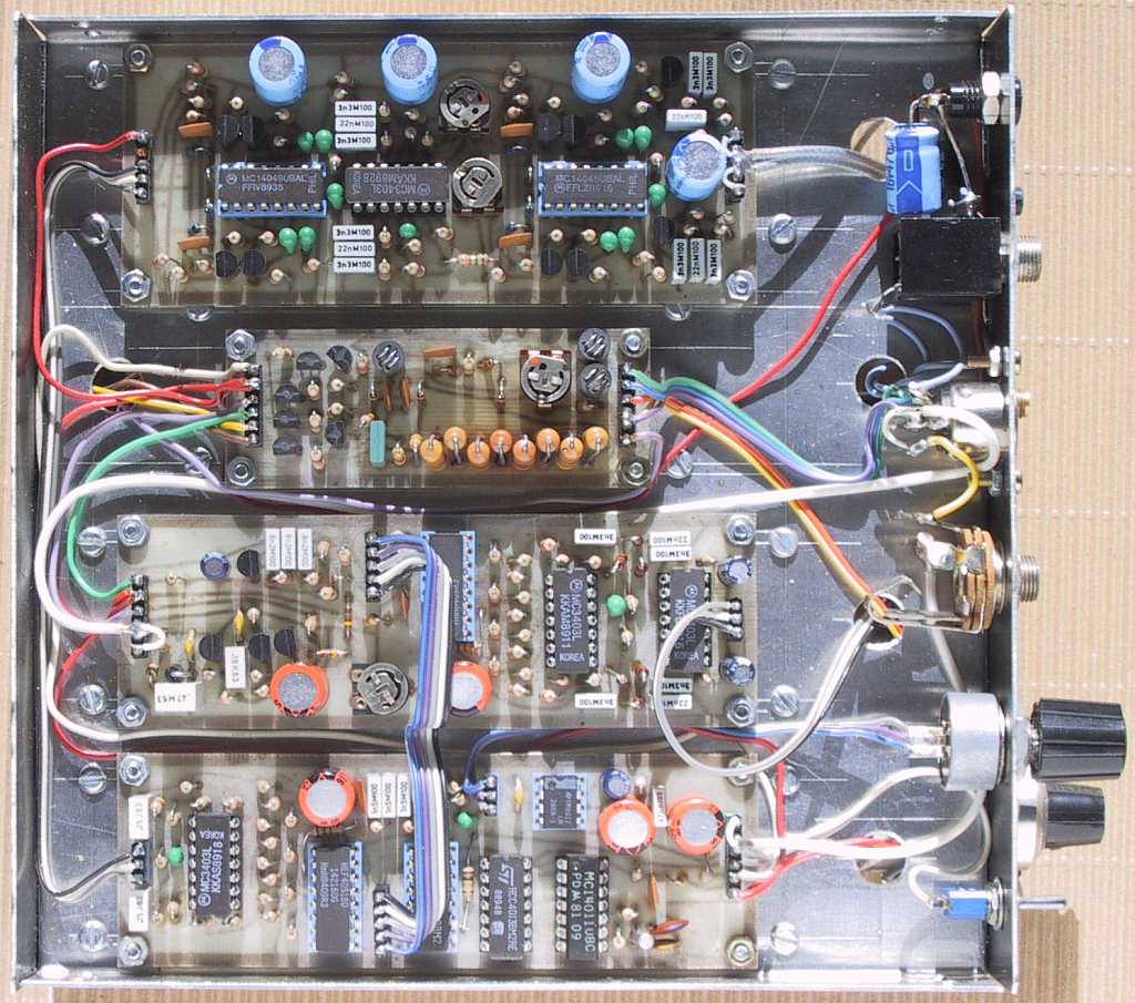
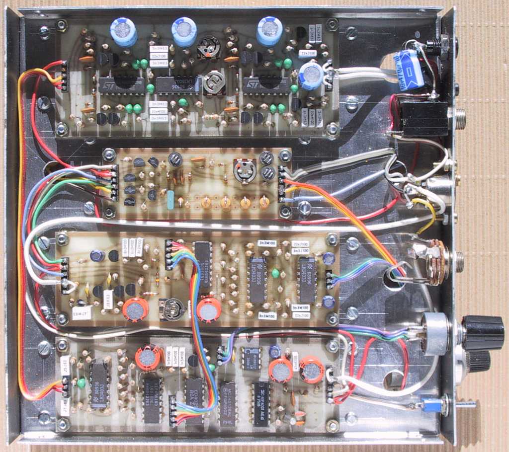
As already mentioned, the IF and AF sections are common to all three transceivers for 23cm, 13cm and 5cm. Their block diagram is shown on Fig.11. To increase the AGC dynamic range, the receiving IF chain has two separate AGC stages. Both include 1.2kHz lowpass filters, discrete transistor amplifiers and MOS transistors (4049UB) used as variable AGC resistors. The receiving IF chain also includes trimmers for gain and phase correction, while no such correction is applied to the transmitter IF chain.
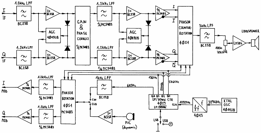
Fig.11 - Block diagram of the quadrature IF/demodulator/modulator/AF section.
The RX/TX switching is not described in detail on the block diagrams. Of course all of the switching is fully electronic with no unreliable mechanical relays. Electronic switching also allows BK CW operation. In the latter case, most RX stages remain active and the receiver also works as a CW monitor.
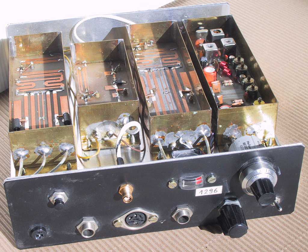
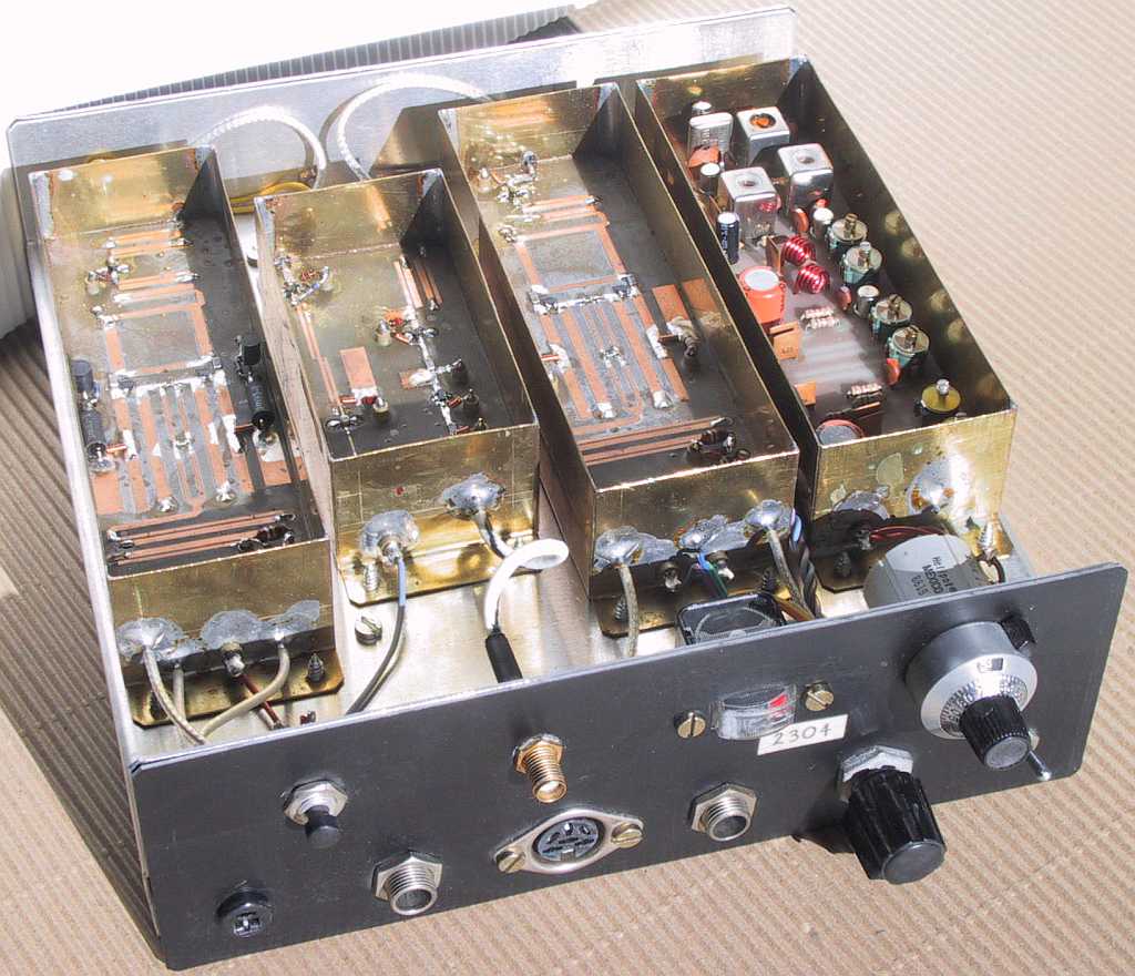
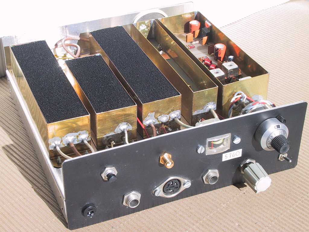
All three transceivers also share a similar mechanical construction. The transceivers are housed in an aluminum enclosure (180mm wide X 180mm deep X 60mm high) divided into two sections by a central chassis plate. The lower section (27mm high) is housing the IF and AF circuits while the upper section (32mm high) is housing the RF units. The RF modules are individually shielded with small brass-plate boxes.