(ZIF SSB)
(1.3, 2.3 & 5.7GHz)
(10GHz)
(3.4GHz)
(24GHz)
(HOME)
NO-TUNE SSB/CW TRANSCEIVER FOR 3400MHz
Matjaz Vidmar, S53MV
1. New frequency band 3400MHz in S5
Since June 1998 amateur-radio operations on the 3.4GHz frequency band were authorized for the first time in Slovenia (S5). Of course we all wanted to activate the new band as soon as possible. The easiest way was to modify the successful and simple zero-IF (Weaver) microwave SSB/CW radios for this band as well.
The 3.4GHz (9cm) band is not very popular among microwave amateurs, at least not in Europe. In ITU region II the amateur allocation extends from 3300MHz to 3500MHz. On the other hand, since a few years ago there were only a few European nations that allowed amateur activity in the 3400-3475MHz segment on a secondary basis. Long-distance narrowband amateur operations were mainly concentrated around 3456MHz both in Europe and in North America, since 3456MHz is a convenient multiple of several common frequencies: 144MHz (x24), 432MHz (x8) and 1152MHz (x3) (local oscillator in transverters).
According to new common European frequency plans, a small part of the 9cm band, usually 3400-3410MHz, was allocated to the amateur-radio service in many European nations. The same frequency band 3400-3410MHz was allocated to the amateur-radio service in Slovenia on a secondary basis as well. Accordingly narrow-band activity in Europe was shifted down to 3400MHz.
Of course the 3.4GHz zero-IF SSB transceiver presented in this article makes use of the proven designs for 2.3GHz and 5.7GHz. The low-frequency and audio stages are the same, as well as the subharmonic mixers with BAT14-099R schottky quads. Besides GaAs HEMTs and INA MMIC amplifiers, the 3.4GHz zero-IF RTX uses new, high-performance and inexpensive silicon bipolar transistors like the BFP420.
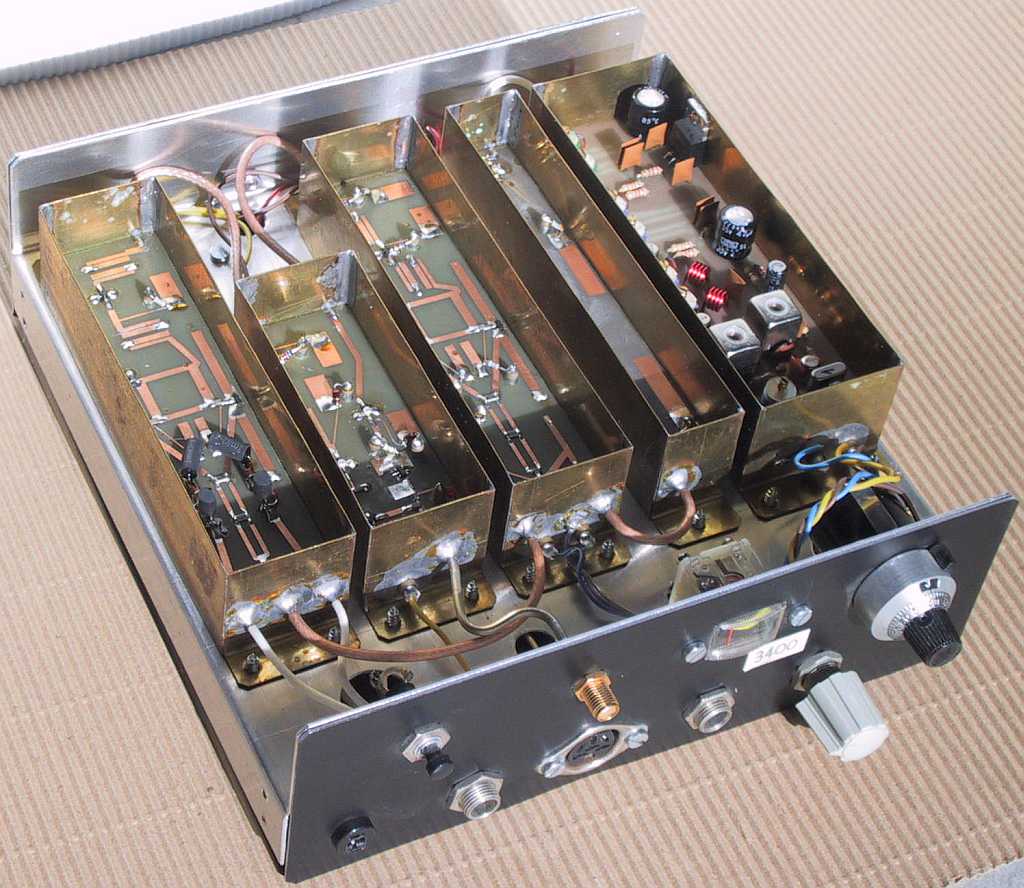
The zero IF SSB transceiver for 3400MHz uses a single PIN-diode (BAR81) antenna switch just like the 5.7GHz and 10GHz versions. Therefore the transmitter output stage (CLY2) makes an integral part of the antenna switch. Although the CLY2 was not designed for operation at 3.4GHz, it can still provide more than 0.5W of output power, although the power gain (8-9dB) is smaller than in the 13cm band. All of the RF stages are built as microstrip circuits on 0.8mm thick glassfiber-epoxy laminate FR4.
2. Modified VCXO and multiplier stages
A transceiver for 3456MHz could use the same VCXO and multiplier chain up to 576MHz as in the 2304MHz version, since the two frequencies are in an exact ratio 3:2. The 576MHz signal is doubled to 1152MHz to drive the subharmonic mixers in the 2304MHz transceiver. The same 576MHz signal could be tripled to 1728MHz to drive the subharmonic mixers in the 3456MHz transceiver.
Since the narrowband segment in the 9cm band was shifted down to 3400MHz, a slightly different crystal has to be built in the VCXO. The above-mentioned frequency multiplications could be used, however they do not represent an efficient technical solution. Above 1GHz silicon bipolar transistors become quite inefficient as frequency multipliers, while GaAs FETs and HEMTs mainly produce even harmonics due to their quadratic transfer function.
The 3.4GHz transceiver therefore includes a slightly modified multiplier chain. The VCXO is using a 17.7MHz (fundamental resonance) crystal. The VCXO output is first tripled to 53MHz, then doubled to 106MHz, again doubled to 213MHz and finally doubled to 425MHz in the same VCXO module. The VCXO module is followed by an additional HEMT multiplier (as in the 5.7GHz transceiver) used to multiply 425MHz by four to obtain 1700MHz to drive the subharmonic mixers.
The modified VCXO and multiplier stages are shown on Fig.1. For operation on 3400MHz, a fundamental-resonance crystal for 17.708MHz is required in the VCXO. Unfortunately this frequency is not standard and a special crystal has to be ordered. The closest standard crystal is the PAL subcarrier multiple at 17.734MHz (used in many TV-sets in Europe) that multiplies up to 3405MHz in the described circuit.
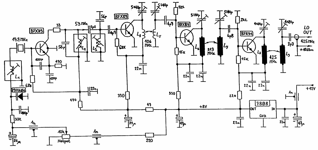
Fig.1 - VCXO and multipliers for 425MHz.
Although narrowband operation is permitted at 3405MHz in all countries where amateurs have access to the 9cm band, it is probably very difficult to find a correspondent on this frequency. On the other hand, if a standard PAL crystal for 17.734MHz is pulled down by 26kHz with a series inductor, the resulting VCXO will not be very stable. In the latter case, just the power-on warm-up frequency drift may reach 50kHz at the final frequency of 3.4GHz.
In order to pull a standard PAL subcarrier crystal down to 17.708kHz, a relatively high series inductance L1 is required in the range of 5...8uH, depending on the crystal used and other parasitic capacitances in the circuit. The stability can be improved by grounding the crystal case. The suggested components (varicap MV1404 and 100pF parallel capacitor) provide a coverage of about 600kHz around 3.4GHz that should be sufficient for narrowband modes including the correction of the VCXO drift.
The multiplier chain is tuned to lower frequencies by increasing the values of the resonant and coupling capacitors, while the inductors are left unchanged. Capacitive trimmers (Philips foil type, 7.5mm diameter with three leads) in the 106MHz and 213MHz bandpass filters are increased to 5-40pF (violet body), while the trimmers in the output stage at 425MHz are increased to 4-20pF (green body).
,br>
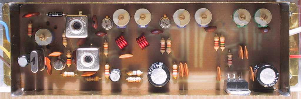
The printed-circuit board of the VCXO and multiplier stages is of course identical as published for the 23cm, 13cm, 5cm and 3cm versions of the zero-IF SSB transceiver. There are only a few changes of capacitor values in the component location, so the corresponding drawings are not published once again. If a standard 17.734MHz crystal is pulled down to 17.708MHz in the described circuit, special care has to be taken that the oscillator operates in a stable way and does not jump on another resonant mode of the crystal.
The circuit diagram of the additional multiplier for 1700MHz is shown on Fig.2. The multiplier includes an ATF35376 HEMT, overdriven with the 425MHz (+10dBm) input signal. The following microstrip bandpass filter selects the fourth harmonic at 1700MHz. The 1.7GHz bandpass is followed by an amplifier (BFP420) to boost the 1700MHz LO signal level to about 10mW (+10dBm).
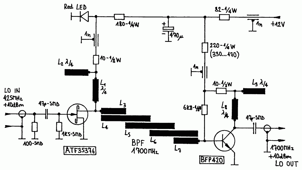
Fig.2 - Additional multiplier for 1700MHz.
The additional multiplier for 1700MHz is built as a microstrip circuit on a double-sided, 0.8mm thick FR4 glassfiber-epoxy printed-circuit board with the dimensions of 20mmX120mm. The upper side is shown on Fig.3 while the lower side is not etched to act as a groundplane for the microstrip circuits. The component location on both sides of the printed-circuit board is shown on Fig.4.
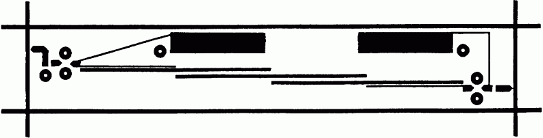
Fig.3 - 1700MHz multiplier PCB (0.8mm double-sided FR4).
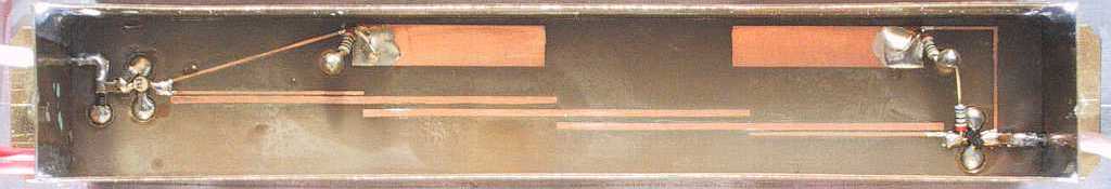
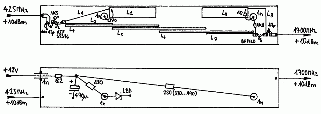
Fig.4 - 1700MHz multiplier component location.
A correctly assembled multiplier for 1700MHz should not require any tuning. One should however check the Idss of the ATF35376 HEMT. When checking the overall transceiver, the LO power level may result too high, degrading both the noise figure of the receive mixer and the carrier suppression of the transmit mixer. In this case it is recommended to increase the supply resistor of the 1700MHz amplifier BFP420 from the original 220ohm up to 330ohm or even 470ohm.
3. Quadrature transmit mixer for 3400MHz
The circuit diagram of the transmit mixer for 3400MHz is shown on Fig.5. Besides two subharmonic mixers, an in-phase LO divider and quadrature hybrid coupler for 3.4GHz the module includes a coupler and buffer amplifier for the 1700MHz LO and two output RF amplifier stages, to boost the output 3.4GHz signal level to about 10mW (+10dBm). All bandpass filters and other passive RF components are built as microstrip circuits on double-sided, 0.8mm thick FR4 glassfiber-epoxy laminate.
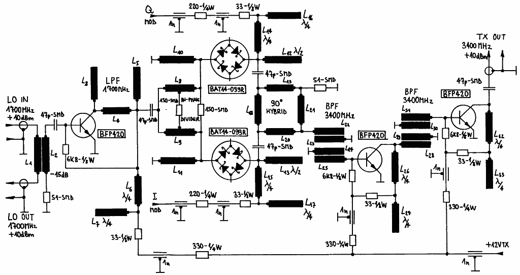
Fig.5 - Quadrature transmit mixer for 3400MHz.
The receiver and transmitter of the zero-IF SSB transceiver for 3400MHz both require the same local oscillator signal at 1700MHz. The switching of the latter is performed in the same way as in the zero-IF SSB transceivers for 1.3GHz, 5.7GHz and 10GHz. Most of the LO signal power is fed to the receive mixer all of the time. A small part of the LO signal is taken by a -15dB coupler and amplified by a BFP420 transistor to drive the transmit mixer. The 1700MHz LO signal is filtered in a lowpass (L3, L4 and L5) before being applied to the two subharmonic transmit mixers through an in-phase divider L8/L9.
The BAT14-099R schottky quads provide a good mixer symmetry at relatively low frequencies, so no special measures are required to improve the unwanted carrier suppression at 3400MHz. Of course the mixer symmetry can be further improved by orienting both BAT14-099R schottky quads in the same direction in the circuit. In practice this means that one of the two BAT14-099R has to be soldered upside down in the circuit.
Both mixer outputs are combined in a quadrature hybrid to obtain the desired SSB signal at 3400MHz. The hybrid is followed by a 3400MHz bandpass (L22, L23, L24 and L25) to remove the LO residuals at 1700MHz and other unwanted mixing products far away from the 3.4GHz frequency band. Two amplifier stages with BFP420 transistors boost the relatively low signal level (about -12dBm) up to about 10mW (+10dBm). Another 3400MHz bandpass (L28, L29, L30 and L31) is built between the two amplifier stages.
The module of the quadrature transmit mixer for 3400MHz is built as a microstrip circuit on a double-sided, 0.8mm thick FR4 glassfiber-epoxy printed-circuit board with the dimensions of 30mmX120mm. The upper side is shown on Fig.6 while the lower side is not etched to act as a groundplane for the microstrip circuits. The component location on both sides of the printed-circuit board is shown on Fig.7.
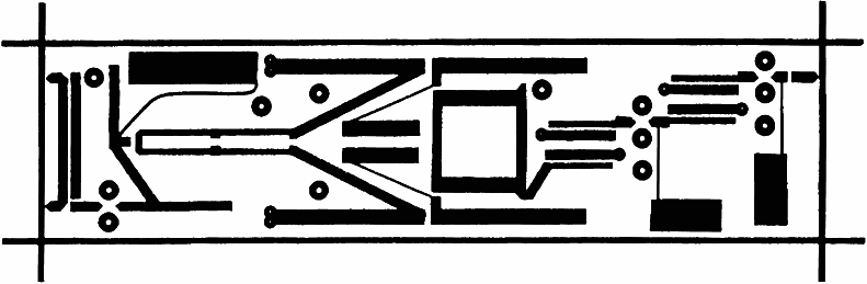
Fig.6 - 3400MHz TX mixer PCB (0.8mm double-sided FR4).
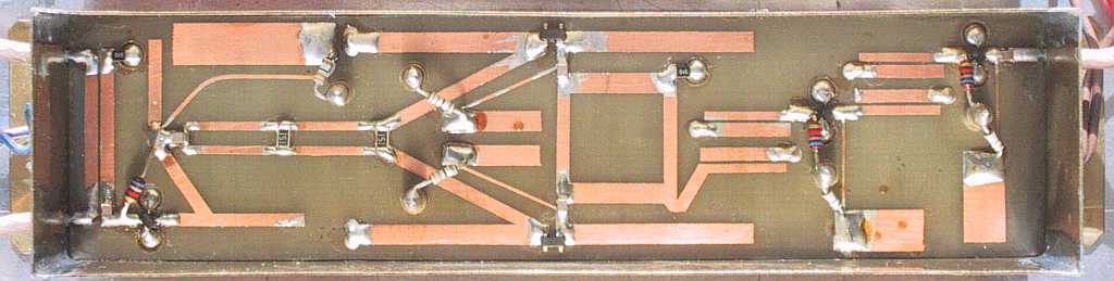
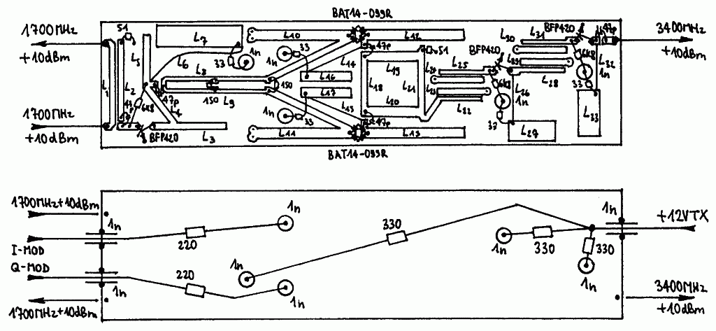
Fig.7 - 3400MHz TX mixer component location.
A correctly assembled quadrature transmit mixer for 3400MHz should not require any tuning. One should however check the output power (+10dBm) and the mixer balance (at least 25dB of unwanted carrier suppression). If the carrier suppression is not sufficient, check the LO power level and the installation of the mixer diodes.
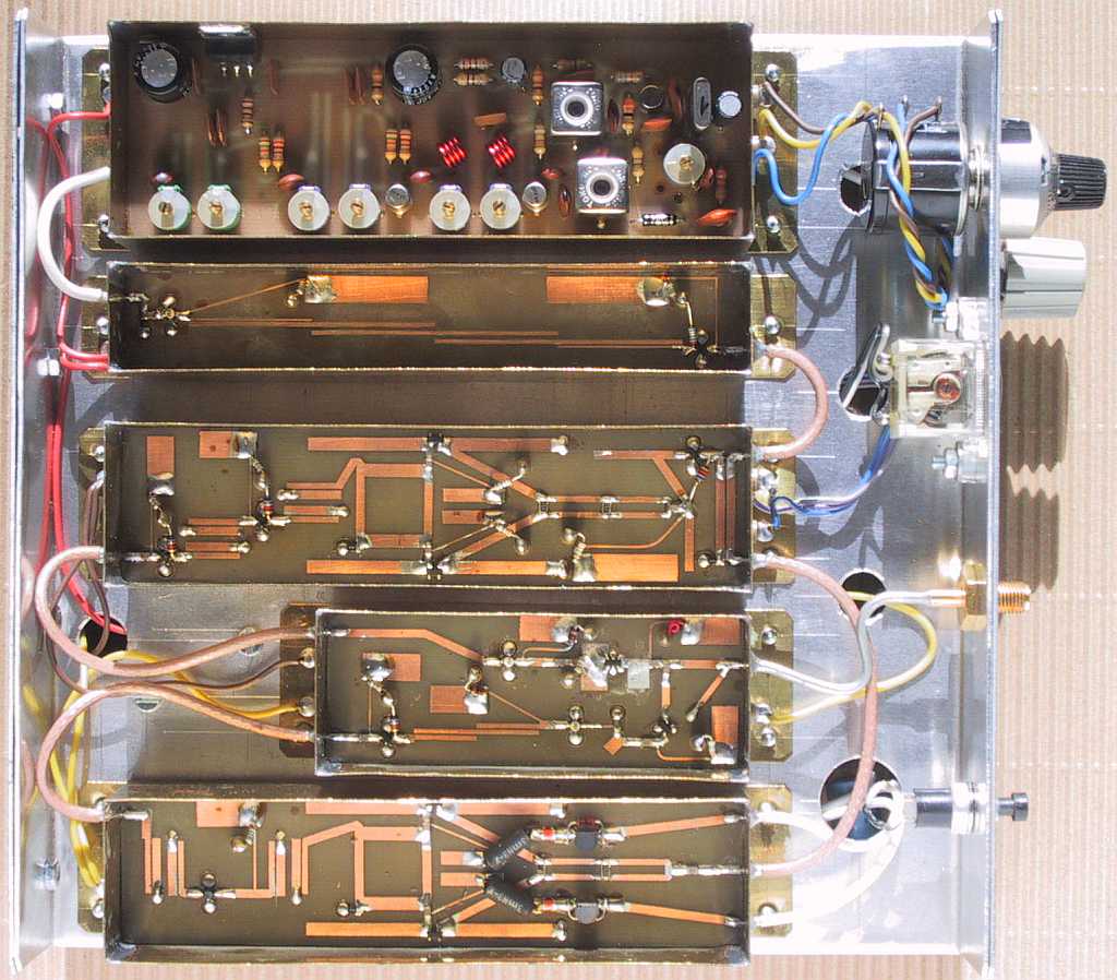
4. RF front-end for 3400MHz
The circuit diagram of the RF front-end of the zero-IF SSB transceiver for 3400MHz is shown on Fig.8. The RF front-end includes the transmitter power amplifier, the receiver RF preamplifier with bandpass filter and the antenna switch with a PIN diode. The RF front-end is built as a microstrip circuit on a double-sided, 0.8mm thick FR4 glassfiber-epoxy printed-circuit board like in the transceivers for 1.3GHz, 2.3GHz and 5.7GHz.
The transmitter power amplifier is designed with the inexpensive GaAs transistor CLY2 in plastic package. The CLY2 can produce more than 0.5W of RF power also on 3.4GHz, however the available gain is much smaller than on 2.3GHz. The gain of the CLY2 amounts to only 8-9dB at 3400MHz and requires a drive power of 60-80mW. An ATF35076 HEMT (high Idss) is used in the driver stage. Since the gain of the ATF35076 is far too high for this application, it is partially reduced by the 100ohm resistor from gate to ground. Anyway, the ATF35076 still provides a few dB of gain margin for the overall transmitter chain.
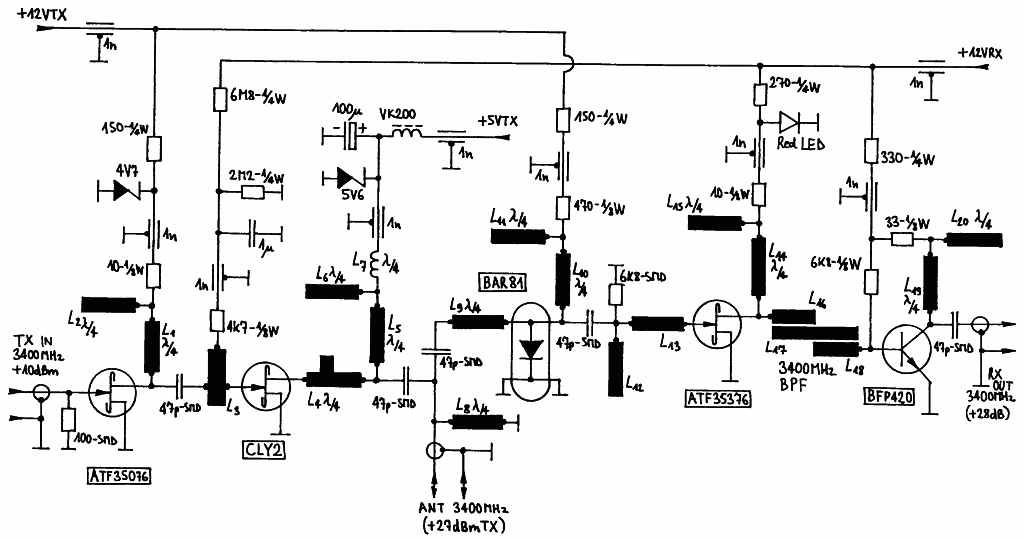
Fig.8 - RF front-end for 3400MHz.
The antenna switch uses a single PIN diode BAR81 in shunt configuration on the receiver input. Due to the low parasitic capacitance of the BAR81, no negative bias voltage is required to bring the diode to the OFF state in the 3400MHz band. No special circuit is therefore required to drive the PIN diode. A simple resistor to +12VTX is sufficient.
While transmitting the short circuit from the BAR81 diode is transformed in an open circuit at the summing node by the L9 quarter-wavelength line. The BAR81 provides more than 20dB attenuation to protect the receiver. On the other hand, the transmitter output stage remains connected to the antenna at all times. While receiving the CLY2 drain voltage is removed and a positive bias is applied to the gate. The CLY2 then behaves as a short circuit, further transformed by L4 in an open circuit at the summing node.
The RF front-end includes a two-stage receiving preamplifier including a simple bandpass for 3400MHz. The first stage uses an ATF35376 HEMT, while a BFP420 silicon transistor is used in the second stage. The overall gain amounts to about 28dB including the losses in the interstage bandpass filter. Since there are no strong signals expected in the 3400MHz band, the preamplifier gain can be kept high to improve the noise figure.
The RF front-end of the zero-IF transceiver for 3400MHz is built as a microstrip circuit on a double-sided, 0.8mm thick FR4 glassfiber-epoxy printed-circuit board with the dimensions of 30mmX80mm. The upper side is shown on Fig.9 while the lower side is not etched to act as a groundplane for the microstrip circuits. The component location on both sides of the printed-circuit board is shown on Fig.10. L7 is the only quarter-wavelength choke that is not printed on the circuit board, but is a small self-supporting coil made of a 25mm long piece of 0.15mm thick CuL wire.
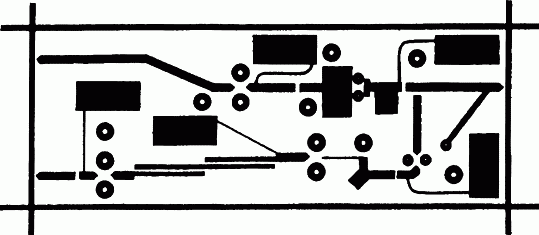
Fig.9 - 3400MHz RF front-end PCB (0.8mm double-sided FR4).
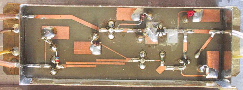
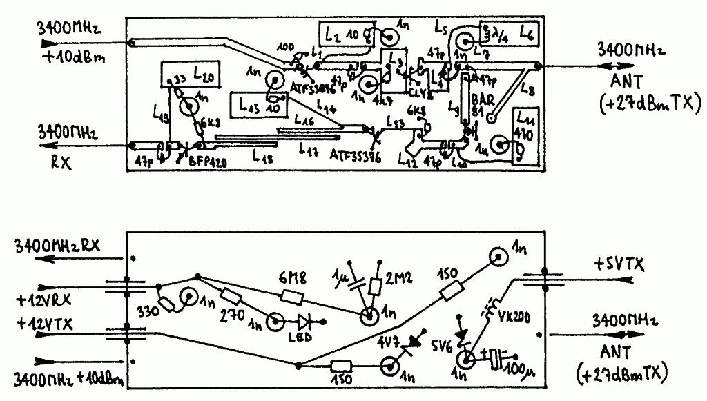
Fig.10 - 3400MHz RF front-end component location.
A correctly assembled RF front-end for 3400MHz should not require any tuning. Before installing the printed-circuit board in the brass frame it makes sense to check the Idss of all of the FETs. Small corrections to the output circuit may bring a few milliwatts more output power, but any improvement is usually less than 1dB.
5. Quadrature receive mixer for 3400MHz
The circuit diagram of the quadrature receive mixer for 3400MHz is shown on Fig.11. The circuit of the quadrature receive mixer for 3400MHz is very similar to the equivalent mixer for 1296MHz except that all bandpass filters, hybrids and chokes are designed for a higher operating frequency.
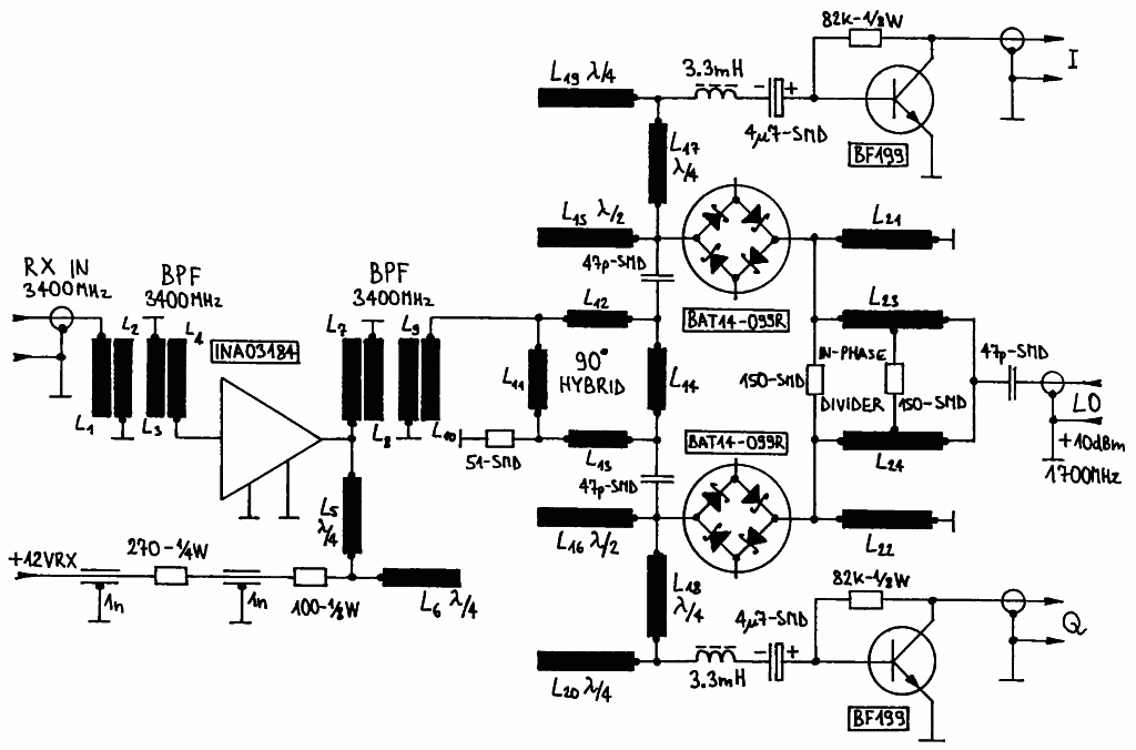
Fig.11 - Quadrature receive mixer for 3400MHz.
Although the available gain from the INA03184 MMIC drops quickly above 2.5GHz, this device still provides the highest gain on 3400MHz with a modest DC current drain. Besides the INA03184 MMIC amplifier, the input signal is fed through two bandpass filters for 3400MHz before reaching the quadrature hybrid. Both subharmonic mixers use BAT14-099R schottky quads, fed in-phase with the 1700MHz local oscillator. Finally, the quadrature receive mixer module also includes two IF preamplifiers with two BF199 transistors.
The module of the quadrature receive mixer for 3400MHz is built as a microstrip circuit on a double-sided, 0.8mm thick FR4 glassfiber-epoxy printed-circuit board with the dimensions of 30mmX120mm. The upper side is shown on Fig.12 while the lower side is not etched to act as a groundplane for the microstrip circuits. The component location on both sides of the printed-circuit board is shown on Fig.13.
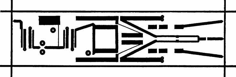
Fig.12 - 3400MHz RX mixer PCB (0.8mm double-sided FR4).
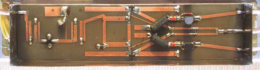
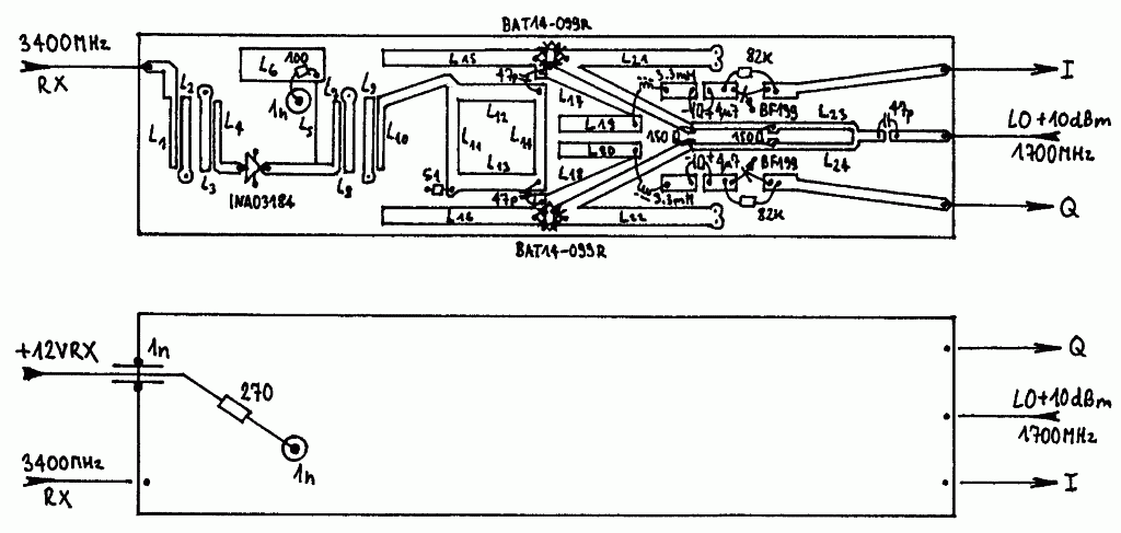
Fig.13 - 3400MHz RX mixer component location.
A correctly assembled quadrature receive mixer for 3400MHz should not require any tuning. Some BF199 transistors may cause excessive "popcorn" noise and may have to be replaced. The mixer noise figure may also increase if the LO signal level is too high.
6. Modification of other modules
The zero-IF SSB/CW transceiver for 3400MHz is using the same quadrature modulator, IF amplifier and demodulator as the (already described) similar transceivers for 1296MHz, 2304MHz, 5760MHz or 10368MHz. The only differences are in the supply circuit for the transmitter power amplifier and in the driver of the PIN-diode antenna switch.
The SSB/CW switching RX/TX module includes a current-limiting resistor for the transmitter power amplifier. The value of the latter should match the RF device used in the particular transmitter output stage. In the 3400MHz transceiver the CLY2 is operated at higher currents than in the 2304MHz version, so the current-limiting resistor has to be somewhat smaller. Recommended values are around 25-27ohm. The exact value is chosen so that the operating voltage of the output stage may rise up to the full value of 5.6V limited by the zener diode in the RF front-end.
The SSB transceiver for 3400MHz does not require a special PIN diode driver like the 5.7GHz and 10GHz versions, since the capacitance of the BAR81 PIN diode is small enough for operation at 3400MHz without reverse bias. However, the abovementioned PIN driver may be required when using higher capacitance diodes like the BAR80.
7. Assembly and checkout of the 3400MHz SSB transceiver
Although the assembly of the SSB transceiver for 3400MHz is not as demanding as the assembly of the 5.7GHz and 10GHz versions, it is recommended to carefully select the components to be used in the RF section. In particular it is recommended to use new SMD capacitors of the size 0805 or smaller, since the older, larger 1206 types may have strange responses in the microwave frequency range. One should absolutely avoid using capacitors made of brown ceramic, since the latter has a high temperature coefficient and high dielectric losses at microwave frequencies.
The 3400MHz version uses a new component, the BFP420 silicon transistor (SMD marking "AMs"). The latter is packaged in the very small SOT-343 package. Also the pinout is changed, since the BFP420 has the emitter grounded internally to improve its RF performance. The wide pin is one of the emitters, the other emitter being located diagonally on the opposite side of the package. The base is on the same side as the wide pin while the collector is on the opposite side of the wide pin. The BFP420 transistors operate at low voltages 2-3V just like HEMTs, but they do not tend to oscillate at very high frequencies like HEMTs.
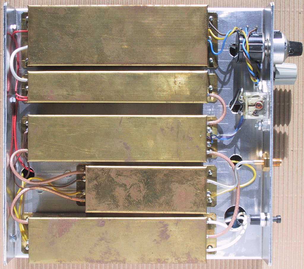
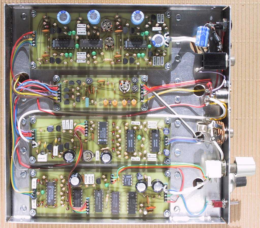
The RF modules of the SSB transceiver for 3400MHz have the same dimensions as the modules of the 5.7GHz and 10GHz versions. Therefore the same brass boxes, overall transceiver enclosure (60mmX180mmX180mm) and module location as in the 5.7GHz or 10GHz versions can be used. The only difference is in the position of some connections, requiring different holes on the brass boxes. All of the microstrip circuits of the 3400MHz SSB transceiver are designed so that no microwave absorber is necessary in any of the RF modules. Also the VCXO module does not require a bottom cover.
The checkout of the transceiver should start with the alignment of the VCXO and multiplier stages. The VCXO should be tuned to cover the desired frequency range. The multiplier stages are adjusted for the maximum output signal, measured as a voltage drop on the base of the following stage. The maximum on 425MHz is found by measuring the drain current (voltage) of the HEMT multiplier for 1700MHz. The additional multiplier for 1700MHz does not require any tuning except for the adjustment of the output power (around +10dBm).
Both the receiver and the transmitter should be already operational, but they still need several checks. In the receiver one should first check the overall gain. There should be a clear drop in the noise when the supply to the LNA is removed and the noise should drop almost to zero when the IF preamplifiers are disconnected. If the drop of the noise power is more pronounced at low supply voltages (10V or less), the LO signal level is probably too high.
Next the receiver is tuned to a weak signal (beacon or another VCXO with multiplier chain) and the received signal is carefully monitored. Besides the main response a mirror signal moving in the opposite direction while tuning should also be heard. The mirror response should be suppressed with the two trimmers in the IF amplifier. Any frequency instabilities are probably caused by the VCXO, especially when using a cheap PAL subcarrier crystal pulled down to 17.708MHz.
The transmitter output power should be checked while adjusting the trimmer in the modulator. In CW mode, the full power should be achieved already at about 1/3 of the full resistance. The supply voltage of the output stage should then rise to 5.6V limited by the zener diode. In SSB mode the output power and supply voltage of the output stage should both drop to almost zero without modulation. The unwanted carrier suppression should be at least 25dB. An insufficient carrier suppression is probably also caused by a too high LO signal level.
The SSB modulation as well as the carrier suppression should also be checked with another station operating in the 3400MHz band. Both LSB and USB have to be checked, since it is relatively easy to swap I and Q lines in the internal wiring of the transceiver. The mode of operation (USB or LSB) of the receiver can also be checked by tuning the receiver to an unmodulated carrier (beacon).
Finally the overall shielding of the transceiver has to be checked. Waving with a hand usually produces a 1.4kHz whistle in the loudspeaker. This effect is common to all zero-IF radios and is caused by the leakage of the LO signal because of insufficient shielding. The frequency of the reflected signal from a moving hand is shifted by the Doppler effect. Finally this signal is collected by the antenna and fed to the receiver front-end.
The current drain of the described SSB/CW transceiver for 3400MHz is about 240mA during quiet reception at a nominal supply voltage of 12.6V. The current drain rises to about 590mA during CW transmission at an output power of 500mW. During SSB transmission the current drain is even higher, since it is inversely proportional to the modulation level, and may reach 750mA during speech pauses.
* * * * *