
(DESIGN)
(COSTAS)
(FRONTEND)
(SUPPLY)
(PCB)
(SHIELD)
(ASSEMBLY)
(TEST)
(HOME)
10Mbps BPSK ZIF transceivers for 1.2GHz, 2.3GHz and 3.4GHz
Matjaz Vidmar, S53MV
4. Supply and RX/TX switching
The three different versions of the BPSK transceiver for the 1.2GHz, 2.3GHz and 3.4GHz frequency bands require many different supply voltages. Most of the low-level electronics operates continuously on +3.3V. The LNA only operates while receiving on +12VRX. The medium-level transmitting stages operate on +5VTX. The 1.2GHz and 2.3GHz transmitting power amplifiers operate on +12VTX. The 3.4GHz transmitting power amplifier requires an additional regulator from +12VTX to +5VTX. All RX/TX supply switching has to be fast enough to avoid slowing down the packet-radio communication protocol, for 10Mbps operation in less than 10 microseconds.
The +12VRX and +12VTX supplies are switched with PNP transistors driven by the /PTT signal (open collector) from the TNC. It is assumed that the TNC includes a hardware watchdog to prevent continuous transmission.
Further the module includes the modulator driver buffering the TXM signal (from the TNC data scrambler) to the appropriate level. The MOD signal is suppressed during reception to avoid unwanted crosstalk. Finally the modulator drive MOD goes through a low-pass filter. The MOD low-pass filter includes two series inductors and one parallel capacitor. The first inductor is located in the supply switch while the capacitor and second inductor are located in the BPSK modulator. The component values are 470nH-330pF-470nH for 10Mbps and 2.2uH-1.5nF-2.2uH for 2Mbps. The MOD signal level is adjustable around 0.5Vpp with a 220ohm trimmer and should have no DC bias.
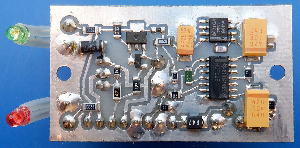
The same switching module was used in earlier BPSK transceiver. It includes a 18V-1W zener for overvoltage protection and two LEDs to indicate RX or TX operation:
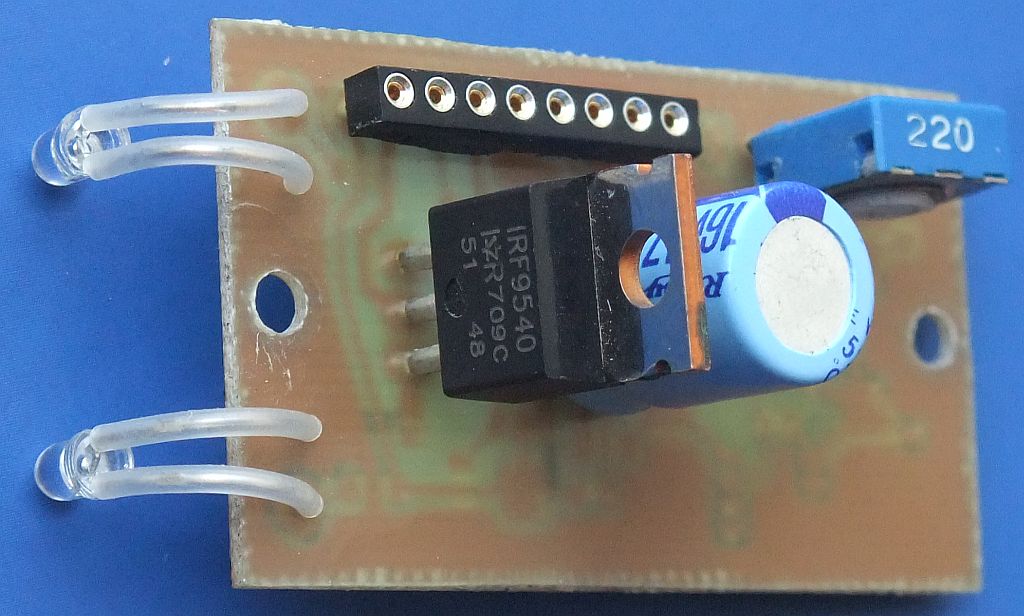
The supply switch is built on a single-sided printed-circuit board to be installed behind the front panel:
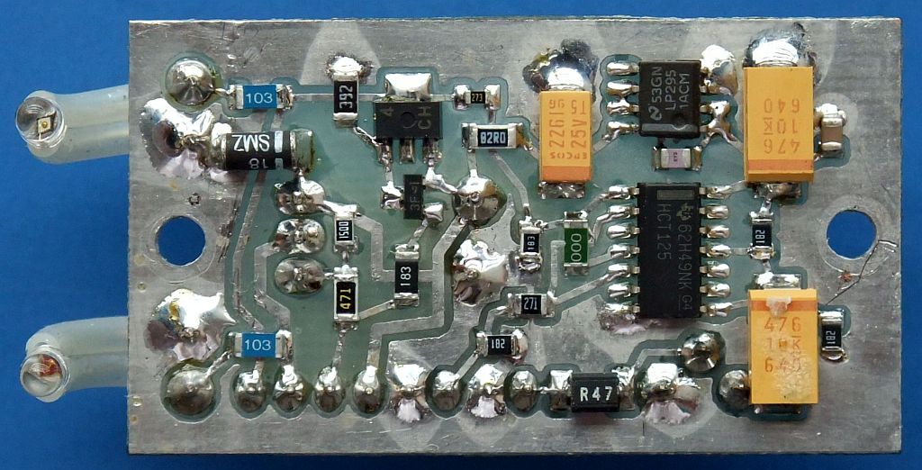
About 10mA can be saved using high-efficiency LEDs and increasing the series resistors form 820ohm to 10kohm:
The BD434 PNP transistor, the 470uF electrolytic capacitor, the 220ohm trimmer, the connector and both LEDs are installed on the top side of the printed-circuit board:
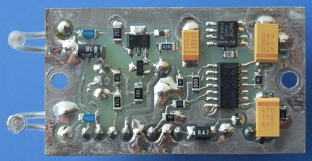
The 3.4GHz version draws a higher TX current that the BD434 PNP switch may not withstand. Therefore the latter is replaced by a more powerful IRF9540 power PMOS switch:

The supply switch is built on a single-sided printed-circuit board to be installed behind the front panel using high-efficiency LEDs:
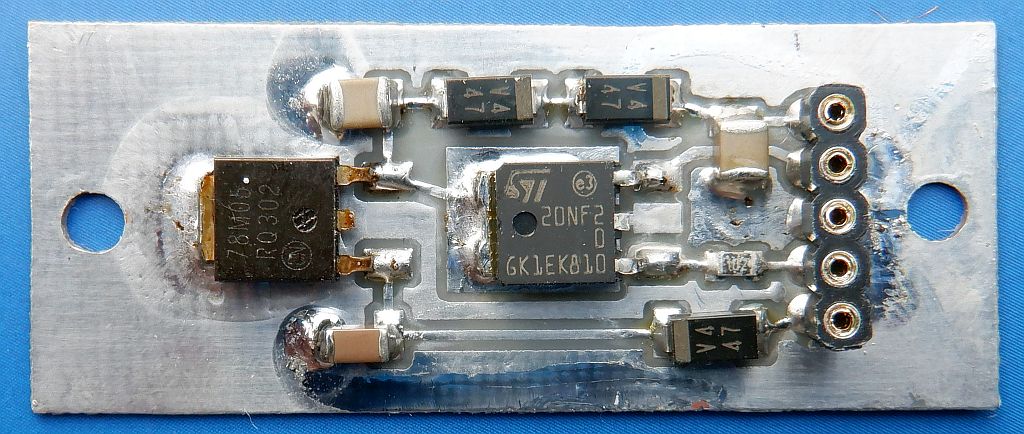
A simple version of the BPSK transceiver includes just a linear regulator 78M05 for both the continuous +3.3V supply and the switched +5VTX supply. The +3.3V supply is obtained from +5V through two silicon diodes. The +5VTX supply is switched with a STD20NF20 power NMOS transistor:

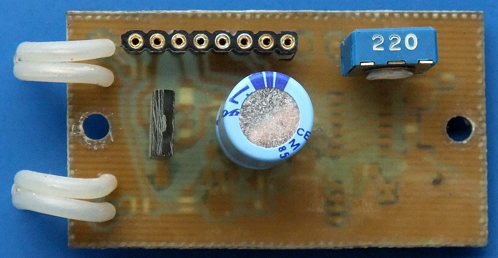
The linear regulator is built on a single-sided printed-circuit board to be screwed directly to the case bottom for cooling, since its total power dissipation amounts to 2.5W during reception and even more during transmission:
The total current drain at 12V of a BPSK transceiver with a linear regulator and standard LEDs amounts to about 280mA during reception and much more during transmission. If a switching regulator is used for +3.3V together with high-efficiency LEDs, the total current drain can be reduced to 100mA during reception. It makes little sense to use a switching regulator for transmission, since most of the current drain is on the +12VTX rail to supply the PTFC270101M power LDMOS.
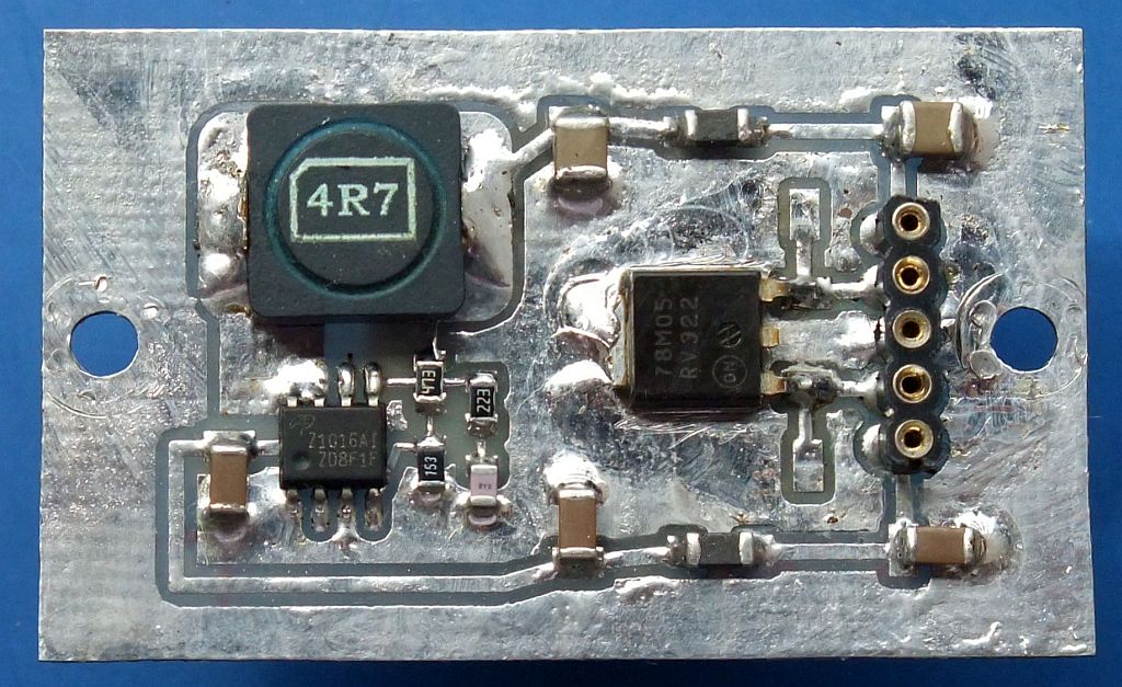
A suitable switching regulator from +12V to +3.3V is the AOZ1016. This IC includes a switching PMOS transistor and schottky diode. Operating at 500kHz it does not cause interference to any circuit of the receiver. The +5VTX supply is obtained from a 78M05 without any input or output capacitors to speed up RX/TX switching:

The switching regulator is built on a single-sided printed-circuit board to be screwed directly to the case bottom for cooling, although its power dissipation is much smaller than its linear counterpart:
The 3.4GHz transceiver requires an additional 7805 regulator in a TO-220 package from +12VTX to +5VTX for the RF front end. Since the current drain of the latter is typically 1.4A, this additional 7805 regulator dissipates around 10W and has to be screwed directly to the bottom of the case. Again no input nor output capacitors are used to speed up RX/TX switching.
(DESIGN) (COSTAS) (FRONTEND) (SUPPLY) (PCB) (SHIELD) (ASSEMBLY) (TEST) (HOME)