The Uncomplicated Universal Usb board
(USB 2.0 interface)
What is it?
- a simple device that brings the power of USB 2.0 interfacing
to the hands of hardware hackers, who don't have the eyes and
fingers to tackle SMD. (Well, khm, I could not completely aviod
the need to do a little bit of SMD soldering, but maybe a keen eyed nimble
fingered friend can do that for you...)
- a simple device that brings the power of USB 2.0 interfacing
to the hands of hardware hackers, who don't want to hassle with
100MB of complicated software just to turn on a single LED.
How did it come to be?
I am a hardware hacker that sooner or later wants to connect
everything to a PC, but the main reason I went into developing this
was my
SIDI interferometer
project for radio astronomy.
In the last couple of years, I've run into two major problems:
1. Good old simple to use interfaces like Centronix, Com ports
and ISA bus are becoming extinct, many new PC's don't have them
any more.
2. With time, my ambitions grew, and I often wanted to pump more
bits faster than these legacy interfaces can swallow.
So it was time for something better and more powerfull.
I read a little about USB 1.1, but it was too slow - if I am
already changing my life with a new interface, I wanted it
to be at least an order of magnitude faster that the ones I
have been using before. Therefore I started
thinking about the PCI bus (and already bought an Xilinx PCI
demo board...) - but then I had some second thoughts:
- PCI is complicated and big and expensive
- it might go the way of the ISA bus sooner than expected
- you have to open the PC to install your gizmo
- it is useless with laptops
Next on my radar was the Firewire (IEEE1394) interface. But the chips
I could find on the web had some unhealthy prices...
Luckily, at that time PCs started to sprout USB 2.0 ports. These
looked promising:
- bandwidth almost in the PCI range
- available on different architectures (will stay popular longer)
- just a thin cable
- available on laptops
- no instalation, just plug in.
After a few days of web surfing, I decided that the Cypress CY7C68013
(AKA "EZ-USB FX2") chip was the best for my purposes:
- can download its own firmware via the same USB bus it is connected to
- has a good set of peripherals (FIFOs, serial ports, I2C, timers...)
- has a reasonable price and is available at many component dealers
the only drawbacks (from my viewpoint) are:
- tiny, fine pitch SMD package
- 3.3V logic
- clumsy Intel 8051 architecture.
- no on-chip A/D (OK, so I am a bit over ambitious :-)
But 3.3V is becoming the new standard anyway, and you can hide the ugly 8051
behind a C cross compiler...
To get around the SMD problem (I want something that plugs easily into
standard 0.254 mm pitch hole-matrix proto boards), I searched the web
for demo boards with this chip.
I found some, but none of them was completely to my liking. For example
the $149
Bitwise QuickUSB board (external link)
uses a special fine-pitch connector - to get normal pin headres, you
must buy an extra $79 "breakout" board.
On the other hand the $89
ELRA usb board (external link)
has a standard pin header, but uses the 56 pin version of the chip, which
significantly reduces the number of I/O pins and interfaces available.
You can get about the same by dismantling an
TRUST Spacecam 380
- these have poor image quality and can be found on Ebay for cca 5 euros...
The board
In the end, I decided to design my own board, which will allow me to use
the Cypress chip with standard pin headers. Luckily, I have a friend
who is skilled at designing and assembling SMD boards, so I drew the
schematic and asked him to do the layout and later solder the tiny stuff.
I chose the 100 pin version of the chip, which brings out all of the
interfaces. There is also an 128 pin version, but that one only adds a
microprocessor bus, which can be used to add external memory to the onboard
8051. I decided that the 8K (a 16K version is also available) of internal
program memory will be enough for my firmware needs. If you need more than
that, adding an external processor smarter than 8051 is a much better idea.
The 128 pin version would just make the board bigger and more expensive.
The board includes only the bare essentials needed to run the CY7C68013,
this way it is the most flexible:
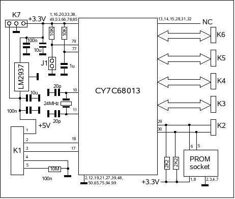
There are more 100n supply blocking capacitors than shown here.
A socket for optional
firmware PROM is included, which can be left unpopulated.
The J1 jumper controls the
wakeup interrupt input and should be left open, if you do not need this
function.
The Tango PCB file of the board in ASCII format is here:
MCPROC1a.PCB
NOTE:The first batch of boards contains an error. Pin 27
"reserved" is not connected to ground. Using cca 10mm of thin wire, it should
be connected to nearby ground.
If it is not, the symptoms are very weird: the xtal oscillator will run, but
there will be no CLKOUT and no attempt to read the EEPROM on the I2C.
It cost me one weekend of banging my head into the wall to figure this out.
When a board with pin 27 not grounded is plugged in, Linux will detect it as
a "full speed" device, and then print a bunch of errors (see "dmesg") as it fails
a few attempts to assign it an address.
Component list
IC1	CY7C68013-100AC	(Cypress EZ-USB FX2)
IC2	LM2937		3.3V regulator  (Watch the pinout!!)
IC3	24LCxx		I2C EEPROM (optional)
Q2	24MHz		HC18SMD   parallel resonant, fundamental, 22pf loading
C1	100nF		1206
C2	100nF		1206
C3	10uF		1206
C4	100nF		1206
C5	10uF		1812
C6	22pF		1206
C7	22pF		1206
C8	1uF		1206
C9	100nF		0805
C10	100nF		0805
C11	100nF		0805
C12	100nF		0805
C13	100nF		0805
C14	100nF		0805
C15	100nF		0805
C16	100nF		0805
C17	100nF		0805
R1	10M		1206
R2	2K2		1206
R3	2K2		1206
R4	10K		1206
R5	10K		1206
J1	2pin header
K1	USB-B connector
K2	3pin header
K3	3pin header
K4	3pin header
K5	40pin header	2row, IDE
K6	40pin header	2row, IDE
K7	3pin header
CY7C68013A (EZ-USB FX2LP) can also be used for IC1. It is a pin
compatible version with lower power consumption and more RAM memory
(16K instead of 8).
When using the CY7C68013A (FX2LP) chip, the following changes must be made:
1. the FX2LP is specified for an quartz crystal with 12 pF loading capacitance
instead of 22pF. (In most cases it will run OK with 22pf, since the exact
frequency is not that important)
2. the rate of rise of the 3.3V supply voltage must be less than 18V/ms.
In other words, the voltage must not reach 3.3V faster than in 200us.
Use a suitable regulator and/or value for the electrolytic capacitor at its
3.3V output.
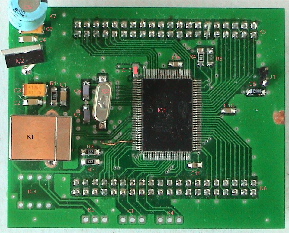
The assembled board looks like this, top side:
and bottom side:
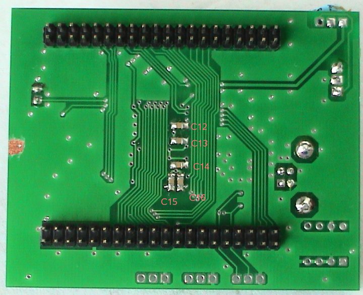
As can be seen, I did not have all components in SMD. Also this is from
the first batch of boards , which contained an error, and the copper wire
that fixes it can be seen on the "top" picture.
A few SMD soldering tips
Assembling the UUUSB board requires some SMD work. An illuminated magnifier
can be very handy with this type of work. Another indispensable tool is the
copper wick for excess solder removal - the finer the wires, the better.
The resistors and capacitors
shouldn't be too much of a problem, you only need suitable tweezers and a
soldering iron with a fine tip.
The 100 pin fine pitch chip is a bit more difficult.
The solder pads are pre-tinned, but if you want to refresh the pads, use the
copper wick afterwards, to remove any solder bumps, that would prevent
the chip from lying flat.
It is very important to position the chip right, precisely aligned on the
solder pads, and prevent it from moving during the soldering process.
First, solder just two pins at opposite corners. This way, the
chip can still be moved a little, by heating one of the soldered pins,
to position it precisely.
Only after the chip is perfectly aligned with the solder pads, proceed
to soldering the rest of the pins!
Start with the pins in the remaining two corners. This way, you cannot
accidentally melt the solder on the two "reference" pins, that you soldered before, and move the chip.
It will be very hard to avoid shorts between the pins, but do not worry,
you will remove them later with the copper wick. Actually, some people just
flood the pins with solder, and later use the copper wick to tidy everything
up.
If you haven't soldered similar things before, I suggest some practicing
on computer junk. Just find some boards with chips in packages similar to
the Cypress. Use a hot-air gun (the type used for paint peeling and shrink
tube shrinking) to desolder them, and then practice re-soldering them back.
Most important, practice your technique with the solder wick!
5V hardware interfacing
The CY7C68013 is a 3.3V device. The "features" page of the manual
says that its inputs are "5V tolerant", but the "absolute maximums"
chapter is somewhat ambiguous - it says 5.25V for inputs and Vcc+0.5V
for outputs in high-Z state. Every bi-directional port pin, when used
as an input, is also an output in high-Z state, so I'm not sure...
To sleep better, I tend to convert any inputs down to 3.3V!
For inputs from 5V logic, resistive dividers can be used.
To bring 3.3V outputs to 5V level, use HCT logic, which sees 3.3V as
a logic one, even when supplied with 5V.
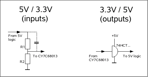
On the input side, the values of the resistors are a compromise between speed
and power consumption. Lower resistance will mean more speed, but
also more power consumed. (Power is only consumed during "high" state.)
The RATIO of the two resistances must always be close to 1:1.51 - for example
R1=10K and R2=15K, to convert from 5V to 3.3V.
Since the lowest resistances you can use depend on the current sourcing
capability of your 5V logic output, you can use a capacitor across the
top resistor to compensate for the input capacitance of the CY7C68013
and the parasitic resistor+wiring capacitances, to get better speed with higher
resistances. The value of the capacitor should be between
a few pF and a few tens of pF. Too big capacitors will cause an overshoot
and could damage 3.3V inputs.
On the output side, if you use HCT for all your external logic, no extra
components are needed for level conversion.
If there is no need to interface with any 5V hardware, one can of course run
all of the external HC logic with a 3.3V supply. However, this will
significantly reduce the speed at which HC logic will operate.
Connectors
The position of the connectors, seen from above, is like this:
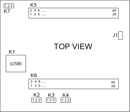
- K1 is the USB "B" connector - here the cable from the PC is connected
- K2 is the I2C interface (3pin header)
- K3 is the first serial interface (3pin header)
- K4 is the second serial interface (3pin header)
- K5 is the high speed FIFO bus (ports A,B,D) (40pin header)
- K6 are the universal I/O pins, timers and interrupts (ports C,E etc) (40pin header)
- K7 are the +5 and +3.3 V supplies from the USB power (3 pin header)
Here are the detailed pinouts of the connectors:
K1:   1 +5V      2 DMINUS   3 DPLUS    4 ground   5 shield


K2:   1 ground   2 SCL      3 SDA


K3:   1 ground   2 TXD0     3 RXD0


K4:   1 ground   2 TXD1     3 RXD1


K5:

 1 ground                 15 PB4  / FD4             29 CTL1 / *FLAGB
 2 PD7  / FD15            16 ground                 30 CTL2 / *FLAGC
 3 PD6  / FD14            17 PB3  / FD3             31 ground
 4 PD5  / FD13            18 PB2  / FD2             32 PA7  / *FLAGD / *SLCS
 5 PD4  / FD12            19 PB1  / FD1             33 PA6  / *PKTEND
 6 ground                 20 PB0  / FD0             34 PA5  / FIFOADR1
 7 PD3  / FD11            21 ground                 35 PA4  / FIFOADR0
 8 PD2  / FD10            22 IFCLK                  36 PA3  / *WU2
 9 PD1  / FD9             23 CLKOUT                 37 PA2  / *SLOE
10 PD0  / FD8             24 ground                 38 PA1  / *INT1
11 ground                 25 RDY0 / *SLRD           39 PA0  / *INT0
12 PB7  / FD7             26 RDY1 / *SLWR           40 ground
13 PB6  / FD6             27 ground
14 PB5  / FD5             28 CTL0 / *FLAGA


K6:

 1 ground                 15 ground                 29 CTL4
 2 RDY2                   16 ground                 30 CTL3
 3 RDY3                   17 ground                 31 ground
 4 RDY4                   18 ground                 32 PC0  / GPIFADR0
 5 RDY5                   19 PE7  / GPIFADR8        33 PC1  / GPIFADR1
 6 ground                 20 PE6  / T2EX            34 PC2  / GPIFADR2
 7 INT4                   21 PE5  / INT6            35 PC3  / GPIFADR3
 8 T0                     22 PE4  / RXD1OUT         36 PC4  / GPIFADR4
 9 T1                     23 PE3  / RXD0OUT         37 PC5  / GPIFADR5
10 T2                     24 PE2  / T2OUT           38 PC6  / GPIFADR6
11 ground                 25 PE1  / T1OUT           39 PC7  / GPIFADR7
12 ground                 26 PE0  / T0OUT           40 ground
13 ground                 27 *INT5
14 ground                 28 CTL5


K7:    1 +3.3V    2 ground   3 +5V
NOTES:
* means active low (inverted)
K7 is a power SOURCE for eventual external circuits with low consumption (<10mA)
DO NOT connect external power supplies here!!
The UUUSB board gets its power from the USB bus!
(If you want to use an external 5V supply to K7/3, cut the line from K1!!)
The I2C bus runs on 3.3V, and the pullups to 3.3V are already present
on the UUUSB board.
DO NOT add external pullups -- ESPECIALLY NOT TO 5V !!!
On pins with multiple functions, which function will be active depends
on what the firmware (you) writes to the internal control registers.
Using the FIFO port
My main reason to start using USB 2.0 was bandwidth. On the CY7C68013 the
interface with the highest bandwidth is the FIFO port.
The other interfaces (serial, I2C, port bits...) are more or less what
one expects them to be, and therefore don't need much explanation.
The FIFO interface on the other hand, is a whole I/O subsystem, and
deserves extra attention.
The FIFO interface on the CY7C68013 is very flexible, and can be operated
in many different modes.

First, it can be operated in either GPIF or SLAVE modes.
The GPIF mode
is a whole world into itself. It includes a state machine, which can be
programmed to perform many different handshakes and simple protocols.
Among others, it can emulate, without additional hardware, interfaces
like Centronix, EPP, ECP, IDE, UDMA, memory card interfaces etc.
In the SLAVE mode, the FIFOs can operate either asynchronously (data transfers
happen on an external strobe signal) or synchronously (there is a continously
running clock, and data transfers happen on its transitions, but only when an
external enable signal is asserted.)
In the synchronous mode, the clock can either be internal (30 or 48MHz) or
external (5 to 48MHz).
In all modes, the clock and strobe/enable polarities can be programmed.
The simplest mode, from the external hardware point, is the asynchronous mode. This
is also the mode that I chose for my first experiments.
Its only drawback is that because of the strobe timing requirements (min 70 ns up,
50 ns down) the maximum frequency at which the data can be clocked is 8.3 MHz (7.1 MHz for 50% duty strobe).
The CY7C68013 contains several FIFOs that can be assigned to four endpoints
(numbers 2,4,6 and 8). But the data for the different endpoints has to be
multiplexed onto the single FIFO data bus that the chip has towards the
external world, and assigned to a specific FIFO by the FIFOADRx inputs.
This is a bit clumsy, so to keep things simple, I tend to only use a single
endpoint for FIFO transfers.
The FIFO port shares pins with ports B and D. Lines FD0...FD7 correspond to PB0...PB7, and FD8...FD15 to PD0...PD7. When a block of data is read, FD0...FD7 comes as the first byte (buffer[0]), FD8...FD15 as the second (buffer[1]) etc. When working on an architecture that stores numbers the wrong way around (INTEL, for example), and you read FIFO data as 16 bit numbers, FD0...FD7 (port B pins) will become the LSB and FD8...FD15 (port D pins) the MSB of the 16 bit word.
Asynchronous write (data input)
As mentioned above, the asynchronous slave mode is the simpest way to
use the high bandwith FIFO interface on the CY7C68013.
The external hardware only needs to provide a simple data strobe to the SLWR
or SLRD input, and set the FIFOADR lines to select the endpoint (when a
single endpoint is used, these can be tied to fixed logic levels).
The data direction terminology is slightly confusing here: asynchronous
write means writing to the FIFO, which is actually reading (data input)
from the viewpoint of the host PC.
The circuit and timing are really very simple:
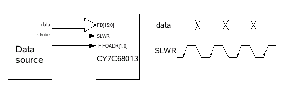
The required setup and hold times (data versus SLWR) are 10ns, and SLWR must be
minimum 70ns high and 50 ns low.
The FIFOADR lines select the endpoint according to the following table:
FIFOADR1	FIFOADR0	Endpoint
   0		   0		   2
   0		   1		   4
   1		   0		   6
   1		   1		   8
Withe the default USB device configuration of the CY7C68013, endpoints
2 and 4 are configured for data output (FIFO read), endpoints 6 and 8
for input (FIFO write).
The CY7C68013 provides programmable full and empty FIFO flags, which can
be monitored by the external hardware to regulate the data flow.
A simple dual channel A/D system
As an example of the UUSB board application, a simple dual channel ADC
system is described here. It employs two 40MHz 8bit A/D converters, but the
asynchronous mode timing constraints limit the sampling rate to 8 MHz.
I've chosen these (TDA8703) A/D converters because theay are available
in the tinkerer-friendly DIP packages.
The schematic is really very simple:
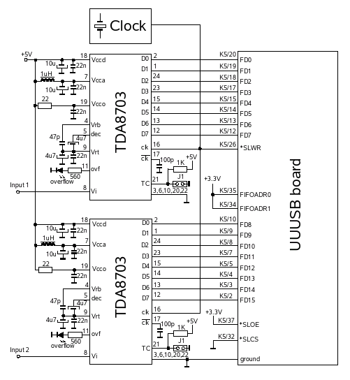
For simplicity, I have just connected the 5V data outputs of the TDA8703s
to the Cypress inputs - so far it has survived.
To reduce the voltage on the TDA8703 outputs to 3.3V it is sufficient to
add 3K3 "pulldown" resistors.
The clock can be either 3.3 or 5V. SLWR is a "pure input" and will
survive 5V, on the other hand TDA8703 will work with a 3.3V clock.
With a 50% duty clock, the clock frequency can be up to 7MHz.
For higher
clocks it would be necessary to switch to
either the synchronous mode (up to 48 MHz)
or GPIF mode (up to 24MHz).
The TDA8703's aren't low power devices, so a separate 5V power supply
is needed to power them. (I don't recommend powering them from the
K7 on the UUUSB board!)
The +3.3V for the FIFOADRx and *SLOE inputs, can be
taken from K7 on the UUUSB board.
The jumpers select between two's complement and straight binary formats.
The analog input voltage range of the TDA8703 is between cca 1.55 and 3.26V.
For first experiments, to see if everything is working, just connect
a potentiometer between 0 and 5V, and feed the wiper voltage to the A/D
inputs.
Of course, for serious use, you will have to provide a suitable analog front end,
with at least the antialias filters and voltage amplification/shifting.
It would be very simple to use one 16bit A/D instead of two 8bit types, but my
interest during development of this was mainly in the direction of interferometry
and simple I/Q software radio experiments, therefore the dual channel version.
Software
Unfortunately, the USB is a complicated standard.
You can use some high-level libraries to simplify its use, but
that way you loose the "real control" on the hardware register
level. Very painful for a hardware hacker.
So I have set myself the goal of clearing away the fog,
and finding simple ways of using USB with full control of the
hardware, at least on the device side.
The software that I wrote for this board is described
here.
Up to S57UUU Home Page
Copyright info