1. The original schematic contains an error in the circuit around U1C, the voltage regulation amplifier. Actual circuits are shown in fig 1.
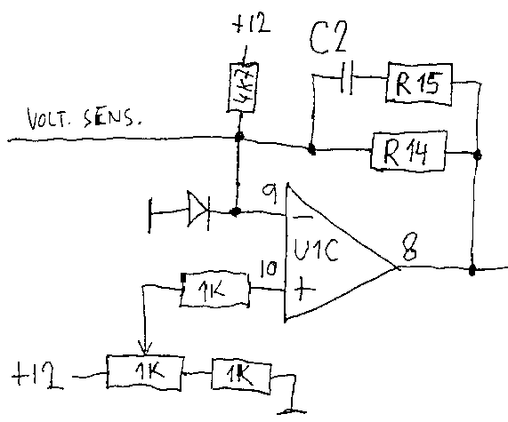
Fig 1a regulated negative voltage
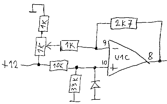
Fig 1b unregulated
The first circuit is for a regulated negative voltage, and the second for unregulated (fixed duty cycle, except for soft start) converter.
2. Depending on the switching thresholds of the CMOS logic, a nasty glitch can appear at the output of the AND gates. It can be removed by level shifting one of the inputs with two resistors, fig 2.
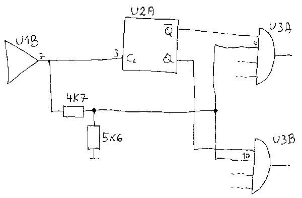
Fig 2 Glitch elimination
3. The transformer configuration that I have proposed in the original paper (secondary sandwiched between two layers of primary) is very bad. I have chosen it on the basis of discussions with some SMPS designers that have told me that the most important thing is to reduce the stray inductances. That is true for low-voltage supplies, but in a HV supply, the main problems are stray capacitances and corona discharge.
In terms of stray capacitance, the thing you must minimise is the amount of energy (U^2 * C/2) stored in it, that has to be pumped in and out every cycle. Since the stray capacitance is distributed all around, it is important to reduce it in the places where high AC voltages exist. Or even better, (because energy increases with voltage squared and only linear with the capacitance) to reduce the AC voltages at the places where most stray capacitance exists. One of the ways to achieve this is to wind the transformer 'high', that is, to use more layers with less turns per layer. For example, if you double the number of layers and reduce the number of turns per layer in half (Figure 3), the stored energy is almost four times less!
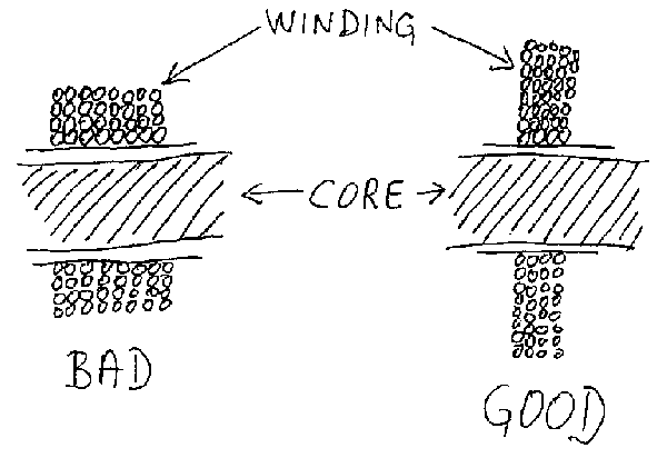
Fig 3. Winding the transformer 'high'
Also, it is good to design the transformer so that parts with high AC voltage are facing outwards. If a rectifier layout as in fig 4 is used,
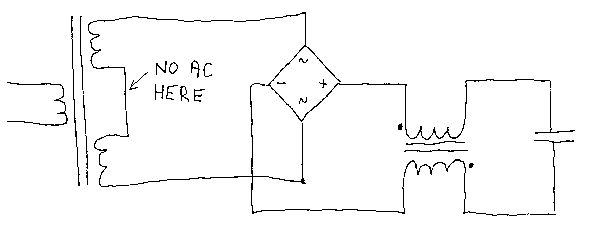
Fig 4. HV rectifier circuit
the center of the secondary winding is AC-wise 'cold'. Then, if the transformer is wound as shown in fig 5, (primary between two layers of secondary or two legs with secondary on top)
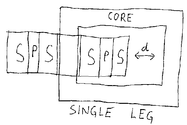
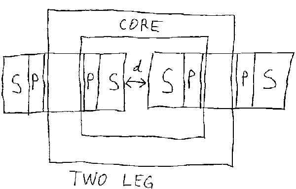
Fig 5. High voltage transformer configurations
there will be no AC over the primary/secondary insulation. The choke is also wound on two legs of an U-core. The wires carying AC (those connected to the diodes) are on the top side of the windings and the wires with no AC (those connected to the capacitor) are on the bottom. Note that the orientation of the windings is also important, as is shown by the dots on the schematic. Depending on the direction of the windings, it is sometimes necessary to invert one of the coils on the core, to simultaneously satisfy both requirements.
Another trick that can help is to divide the secondary in several sections, each with its own rectifier, as I have done in my original design. However, there are many variables and possible configurations of this circuit, not all of them good!
Corona appears at places where high AC fields are present, that is also where most of the capacitive energy is stored. So the same measures that reduce stray capacitance problems also reduce corona problems. In the single leg design of the transformer, corona will tend to appear inside the coil, between the coil former and the core, and if the winding is too high, at the place where it comes close to the other leg. In the two leg design, corona will appear only in the middle, between the two windings. Corona can also appear between the two coils of the choke. To fight corona, I have in both cases inserted PTFE sheet between the coils and filled the remaining space with silicone.
It is important to fill all the space, since corona will appear in air pockets and eat away at the insulation.
4. I have found out that it is very hard to achieve PWM voltage regulation in a high voltage low current supply without using BIG (tens of watts) bleeder resistors. Because of the parasitics, the capacitors tend to peak charge if there isn't enough load current. Therefore, I will change my design so that for the helix supply, where the current is low and the regulation is important, I'll use a fixed duty cycle converter with a pre-regulator. This way, voltage multiplication with diode/capacitor networks is also posssible, reducing problems with the transformer. (Well, NOW I REALLY KNOW why most of the other guys do it this way :-).
I haven't yet finished this version, so I cannot give the schematics here - but I must leave something for the next conference anyway, HI.
Reference:
Marko Cebokli: A TWT POWER SUPPLY, '96 EME conference Bowie MD, USA