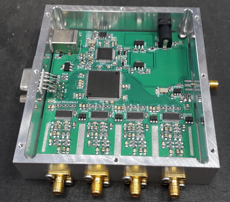
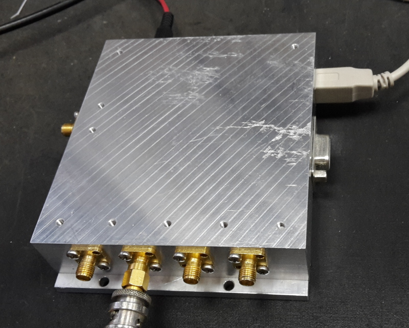
SISA - The SImple SAmpler
I like to play with multiple (receiving) antenna setups, like interferometry,
so I need multi channel receivers.
In the past I used USRP1, which could be setup with four inputs, but it is not
being produced any more.
I did not like other multi channel solutions available on the market, they were either
low performance or expensive, so I decided to roll my own - and also to learn
programable logic while doing it.
My requirements were:
-at least 12 bit sampling
-at least 64 MHz sampling
-low crosstalk
-stable phase
-being hand solderable (no BGAs)
-built on a simple two sided PCB less than 10x10cm in size (cheap!)
-some auxiliarry inputs/outputs (I2C / SPI synthesizer control etc.)
Slides (in Slovene) from a presentation that I gave at a HAM meeting in S5 are here:
RIS2020.pdf


Hardware
The whole thing is open hardware.
Schematics in PDF format are here:
sisa1.pdf
Gerber files for PCB production are here:
sisa1_gerber.zip
Assembly files (BOM, positions...) are here:
sisa1_assembly.zip
The whole KICAD project is here:
sisa1_kicad.zip
Warning: Fake crystal oscillators !!
In a high speed A/D conversion system, the phase noise
(jitter) of the clock is very important.
Lately, it has become hard to find the real good crystal ocillators
among all of the impostors! Here I list three that should be avoided, because of their
lesser signal quality.
Synthesizers masquerading
As it became possible to integrate the VCO onto the synth chip, synthesizers became so
small, they could hide inside crystal oscillator packages. Instead of grinding a
selection of different crystals, it is cheaper for the manufacturers to just make one,
and hide a synthesizer into the oscillator package. These are called
"programmable oscillators". When their phase noise plot is shown in the datasheet, the
"synth shoulder" can clearly be seen.
MEMS oscillators
MEMS technology has advanced to the point, where mechanical resonators can be etched
on a silicon chip, together with the oscillator active circuits. This is of course
cheaper than making a separate quartz crystal, but also means worse performance.
And, as could be expected, MEMS + synth chips came soon after.
"Spread spectrum" oscillators
To add insult to injury, some oscillators are iintentionally made wobbly.
Remember the story with VW diesel cars, that detected when they were tested, and cheated?
These oscillators are made to cheat the EMC tests. Sadly, they are not smart enough
to know when they are tested, so they are just bad all of the time.
So, what to buy?
I strongly recommend the EPSON oscillator I specify in the BOM. Else, only buy
oscillators that have phase noise and/or jitter specified in the datasheet, and compare
it with the recommended EPSON oscillator.
Software
As usual with me, firmware and host software are lagging a bit.
It is all GNU GPl v2 libre software.
FPGA firmware
First, the FTDI chip must be set to FIFO mode. This can only be done with an external
EEPROM (U301 in our case). To set the chip into FIFO mode, I have modified the "eeprom"
program from the libftdi examples collection.
To display the eeprom contents just do
./eeprom
to wite the FIFO configuration, do
./eeprom -w
The program is here:
eeprom.c
(needs the libftdi library),
and a compiled version (linux64) is here:
eeprom
I've made a basic FPGA firmware, that samples and down converts four A/D channels, and
packs them for transport over USB. Both FPGA and A/D converters run from a 64MHz clock.
Decimation is fixed at 64x, so the output sample rate is 1MHz complex (1MHz bandwidth).
Samples are 16 bit I and 16 bit Q for each channel. Together with headers and metadata,
this is a little more than 128 Mbit/s over the USB (less than 50% of the theoretical USB2
bit rate).
It uses all of the DSP blocks in the FPGA, other resources are on average 50% utilized.
Using clock doubling inside the FPGA would allow even better FPGA utilization
(ISE calculates a max possible clock around 170MHz), but the
clock wizard in my ISE installation is broken.
The DDC LO frequency can be set via USB. Currently, the same LO is used for all four
channels, but it would be trivial to give each channel it's own LO.
The binary FPGA configuration file is here:
sisa1_4c.bin
The whole ISE project is here:
sisa_4c_ISE.zip
This is more or less my first serious FPGA project, so the code is ugly and clumsy -
when compiling, ISE reports hundreds of warnings (including "102% device utilization"),
but in the end, it spits out something that works.
Host software
Here is a simple test program, that reads the samples from the SISA, and displays
four spectrums:
testsisa.zip
The zip file contains both the source and a compiled executable (Linux 64bit).
The FPGA config binary is also included.
The program uses Xlib graphics, so it probably won't run on Wayland systems.
It uses a lot of stack space, so you may need to do
ulimit -s unlimited
to avoid segfaults.
It is a simple single threaded program, the FFT and drawing functions are called directly
from the USB callback. In a more serious program, the callback should just write the
data into a circular buffer, for another thread to process. Nevertheless, on a decent
machine (like my old I5 HP ProBook 5650b laptop) it should run practically without
lost packets. even when some other lightweigt software is running along.
It tries to lock itself into memory and switch to real time scheduling, to further
reduce lost packets. It can only do this, when running as root. Otherwise it will
print out a complaint, but will continue to work with normal priority.
Some results
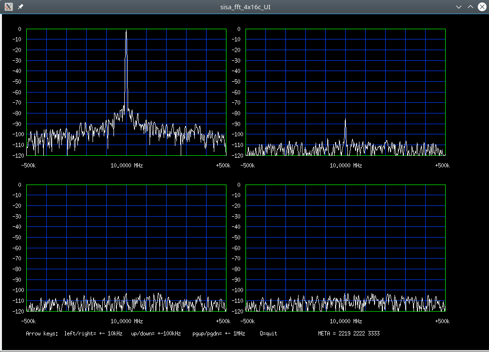
For the first test, I set an HP33120 to 10 MHz and connected it to channel 0.
Then I set the maximum undistorted amplitude (3.3Vpp).

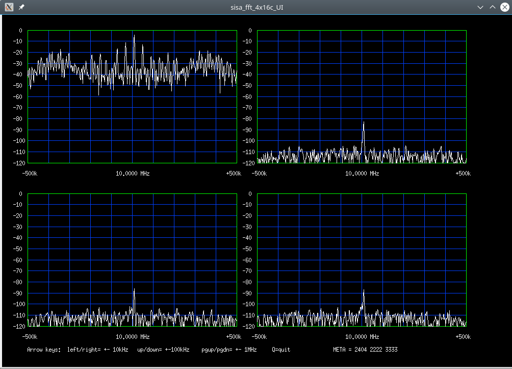
These A/D converters don't take overload well. Just a slightly higher amplitude (3.4Vpp)
results in this:

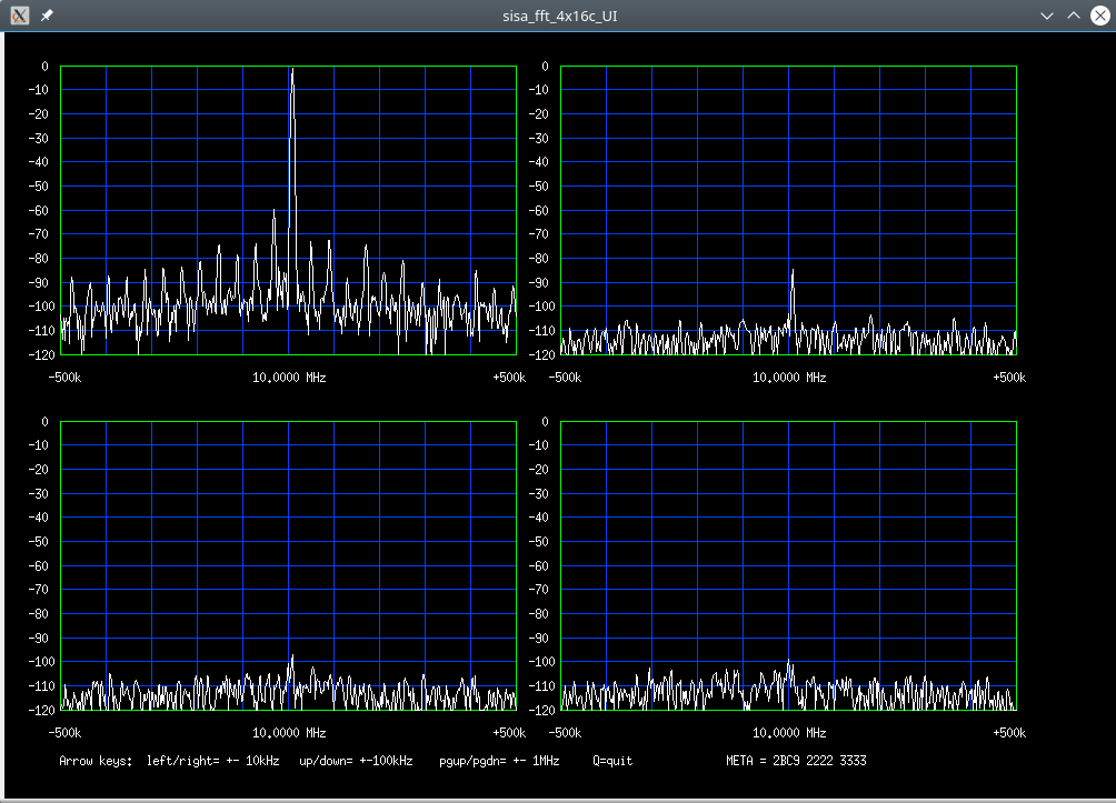
Next, I went back to 3.3Vpp, but changed the frequency up by 10 kHz:

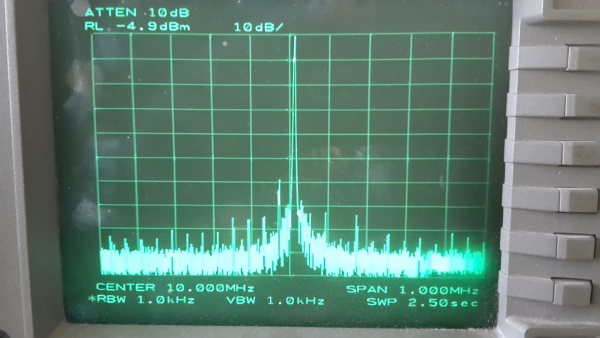
Oooops! What is this? So I connected the HP33120 to an analog HP8563E analyzer:

Good! These lines are real! Obviously, we need something cleaner to test this baby!
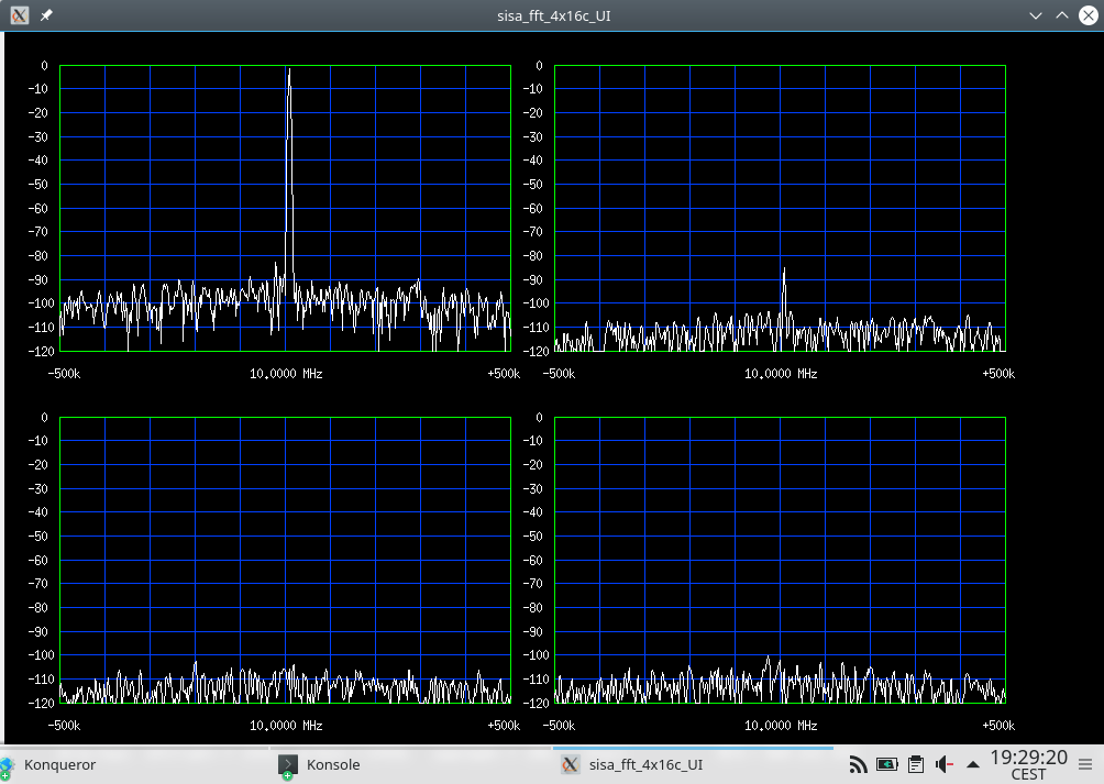
So, my HP8663 had to jump in:

That looks great.
But what are the maximum spurious responses over the band?
I still need to measure this. It won't be easy, the AD9235 is specified at -85 dBc,
and it is not easy to get such a clean signal! The harmonics can alias down, etc.
I will have to make some filters...
Apart from the A/D, there will of course be some images and aliases from the non-ideal
CIC and FIR filters in the FPGA. I had to use shorter CIC filters, to squeeeze
everything in with the FPGA running at fundamental frequency. (Must get that frequency
doubling to work...)
So for now, I expect something like -60dBc max spurs within the 0...32MHz band.
Up to Misc HAM Page
Up to S57UUU Home Page
