| Kenwood TS-820(S) "aftermarket" frequency counter
Back to S56AL main page!
|
|
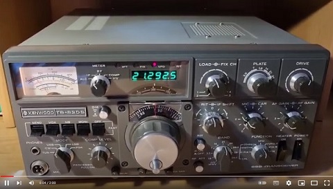
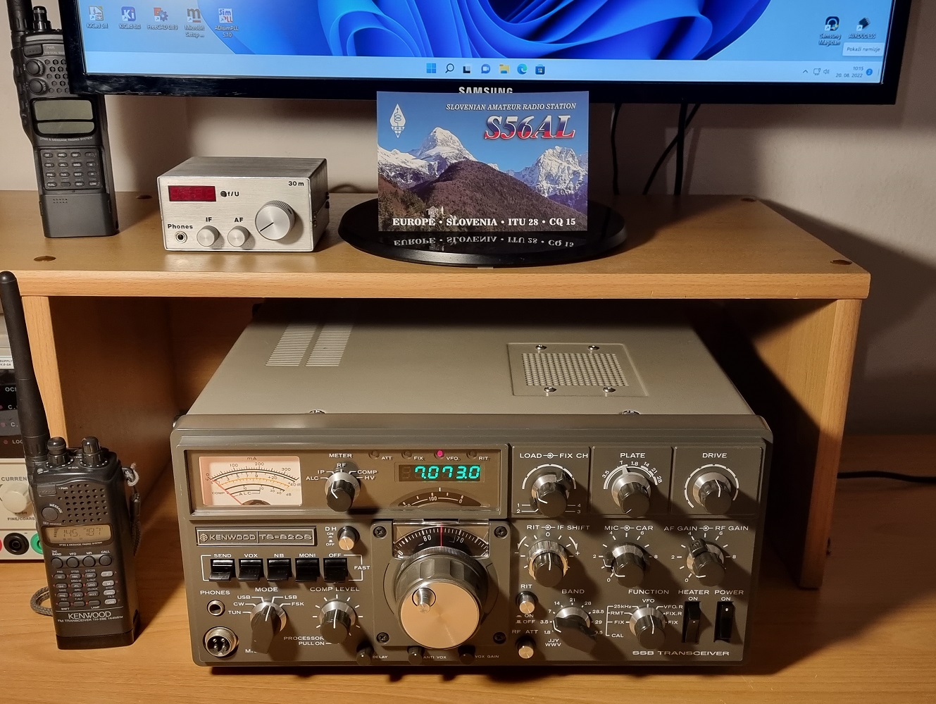
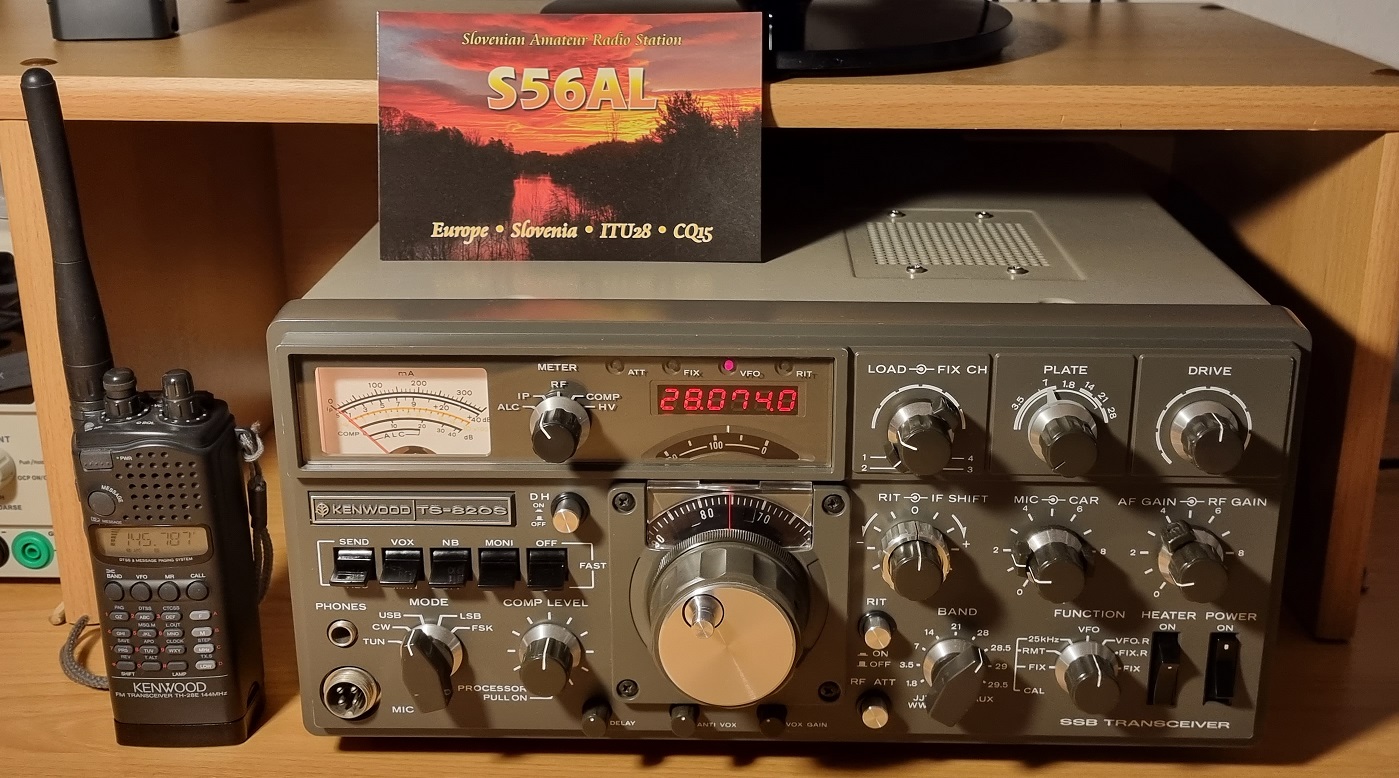
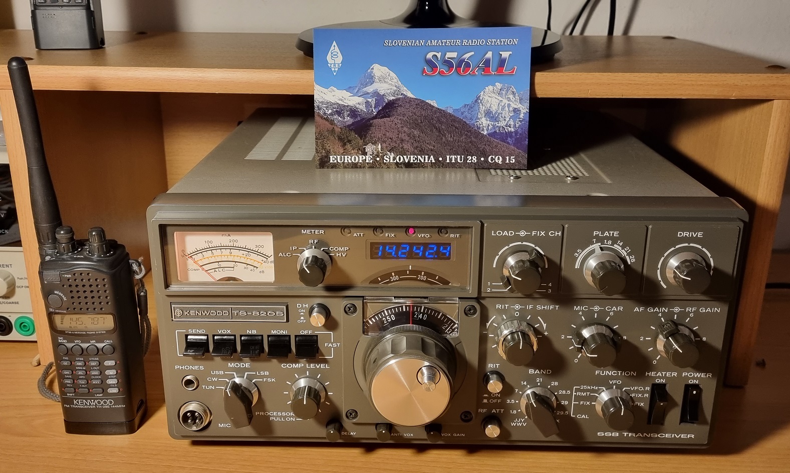
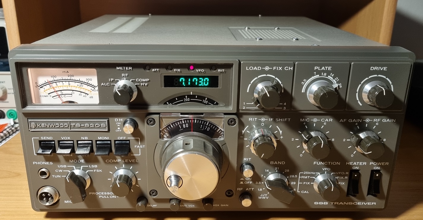
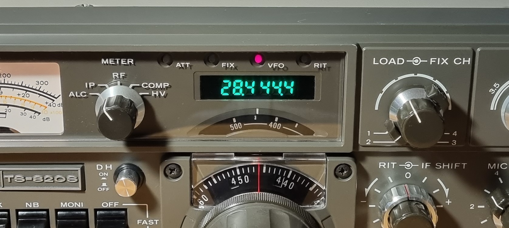
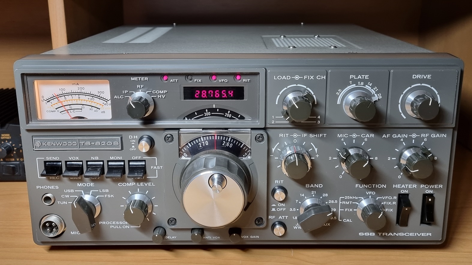
A while back I was fortunate enough to come across a classic, the Kenwood TS-820S "Hybrid" transceiver in relatively good condition. Unfortunately, the frequency counter originally built into the "S" version was missing. After consulting with two HAM colleagues, TS-820 owners who were facing a similar problem, the decision to build an "aftermarket" frequency counter to match the TS-820(S) was an obvious one. The current result of the efforts can be seen in the images below as well as the video above.
Let me point out that this is not a commercial product. I do not sell either built devices or KITs!
 |
 |
 |
 |
 |
 |
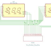
Dual-input frequency counter
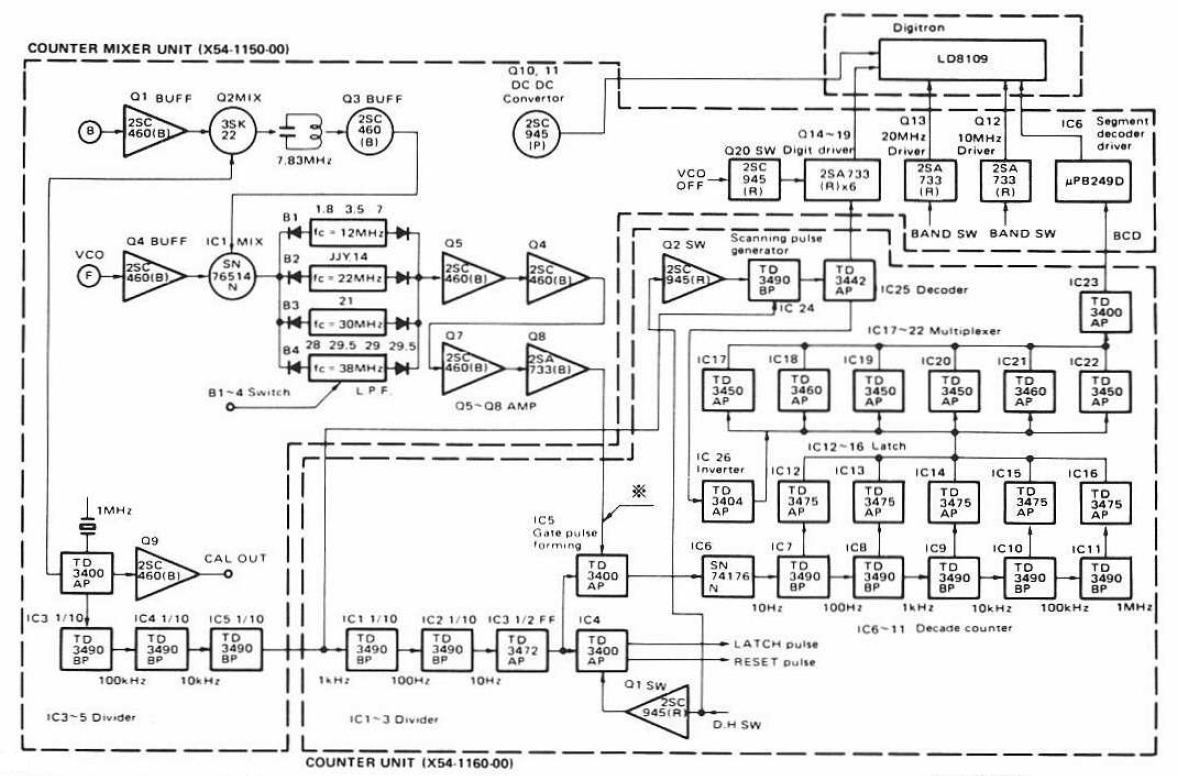
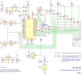
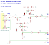
The Kenwood TS-820(S) frequency counter is basically a dual input device. The principle of operation of the original counter, developed and built into the TS-820(S) by the manufacturer, is shown in the block diagram below (left).
 |
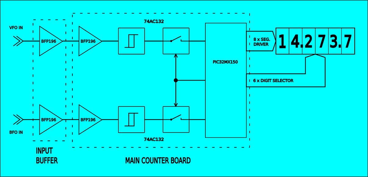 |
To put it simply, in the original frequency counter the two output signals from the VFO and BFO are being mixed in analog harmonic mixer. The resulting output signal is processed by switched bandpass filters to remove all mixing products except the frequency difference. The remaining signal is fed to a frequency counter, measuring and displaying the VFO - BFO frequency difference on a 6 digit 7 segment display.
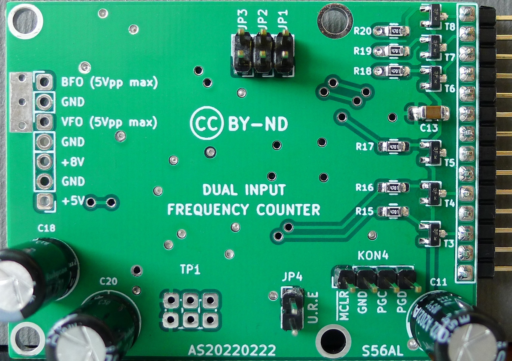
The implemented concept of the frequency counter, described above, coresponded to the era the TS-820 appeared on the market. However, the microprocessor and microcontroller technology has advanced significantly since then. Using a present day technology all necessary tasks may be performed in a low cost single chip 32 bit microcontroller. A 44 pin device like a Microchip's PIC32MX150 entry level 32 bit microcontroller is well capable of counting two frequencies (BFO and VFO) simultaneously, substracting the obtained results from each other as well as driving the 6 digit 7 segment LED display in a multiplexed mode to display the transceiver's operating frequency. Last but not least, the total current consumption of up to 80 mA is way below the consumption of the original counter, built of traditional TTL logic ICs.
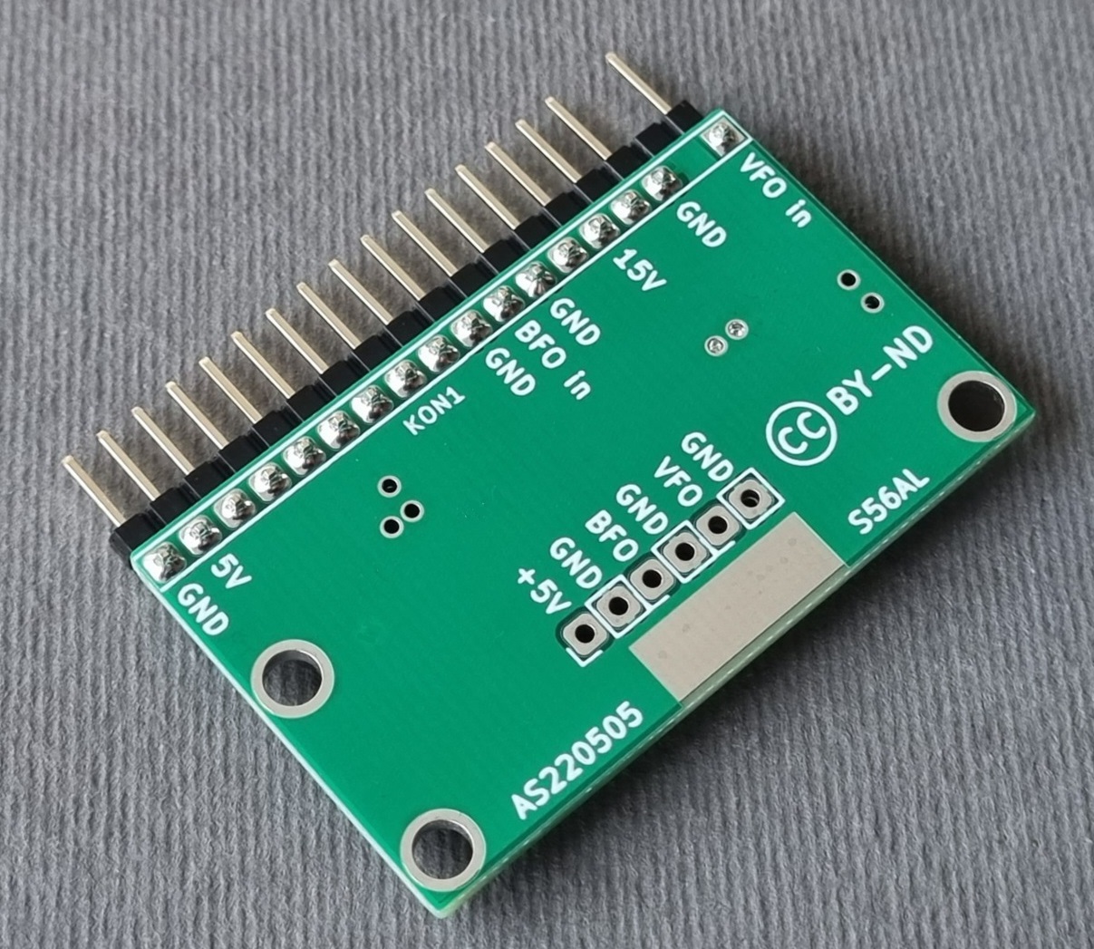
Version 2.2 - release February, 2023
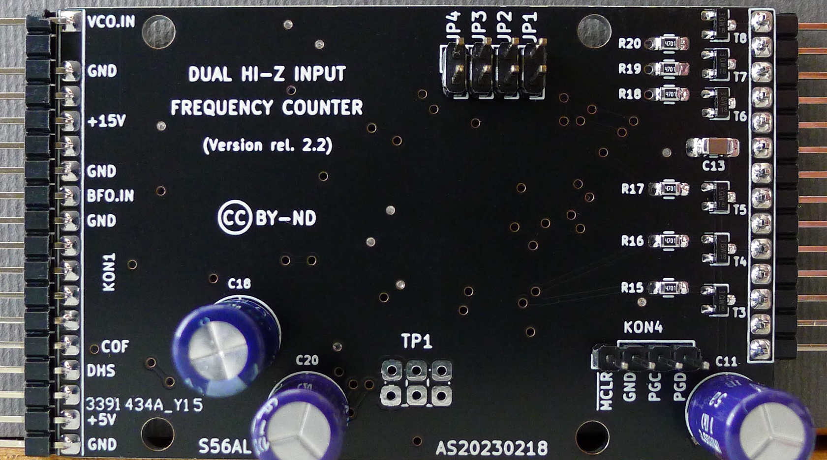
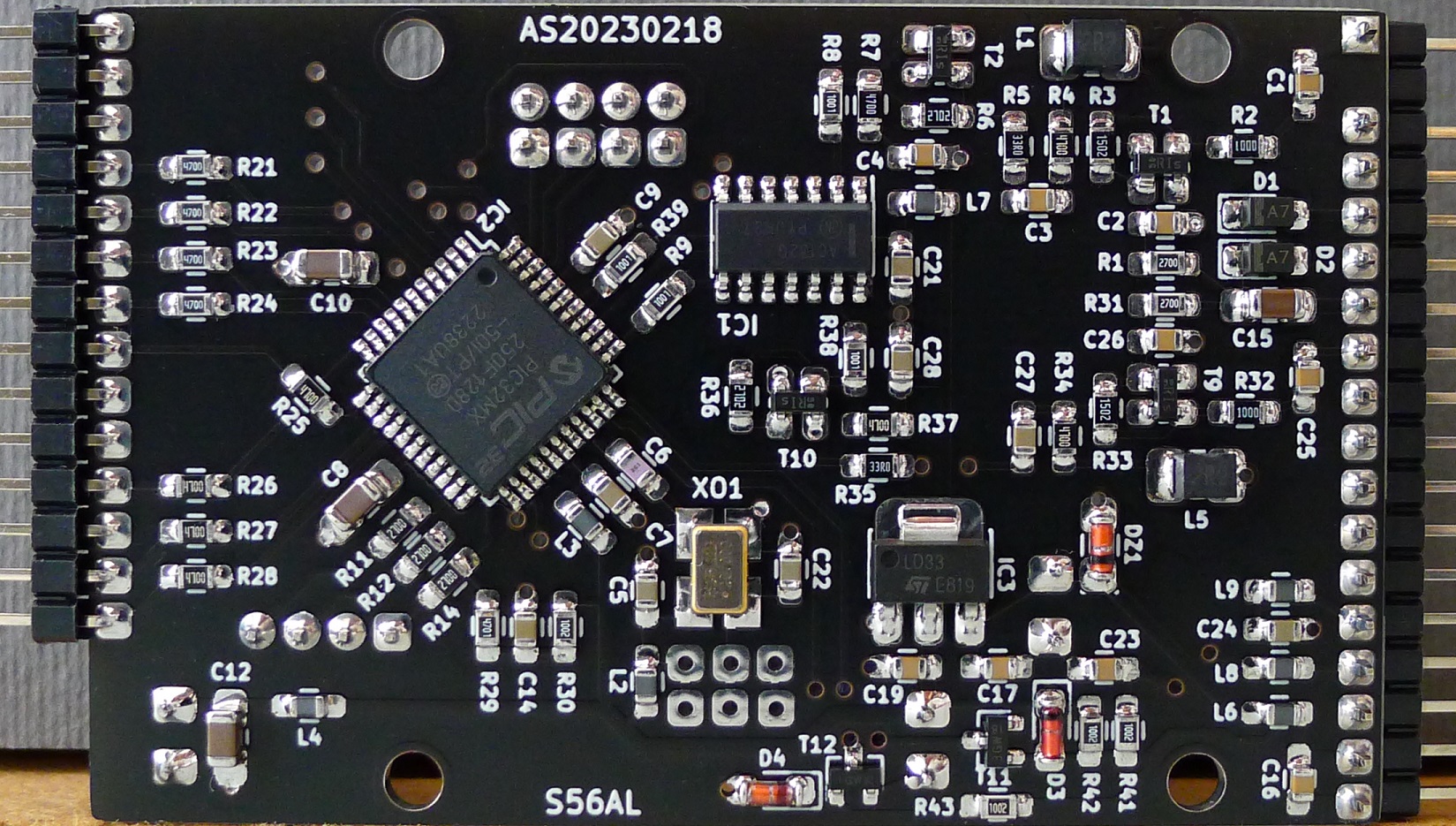
The V2.2 release of the frequency counter engages another PIC32 microcontroller family member (...MX250F128D) which seems to remain available from the major components suppliers in small quantities despite the all-present semiconductor availability crisis experienced in the recent few years. The schematics has been adjusted to set free the microcontroller pin 10 (port RB.12) and pin 42 (port RB.6) dedicated to the USB bus exclusively in the "...MX250F128D" family member and engage ports RA.10 & RC.1 (pins 12 & 26) instead.
The printed circuit board and the embedded software (firmware) were adapted accordingly as well. Other than that, nothing else has changed.
 |
 |
 |
| PCB layout Ver. 2.2 - Gerber files (99 kB - zip) | PIC32 programming file Ver. 2.2 (hex 5 kB - zip) |
Version 2.1 - release November, 2022
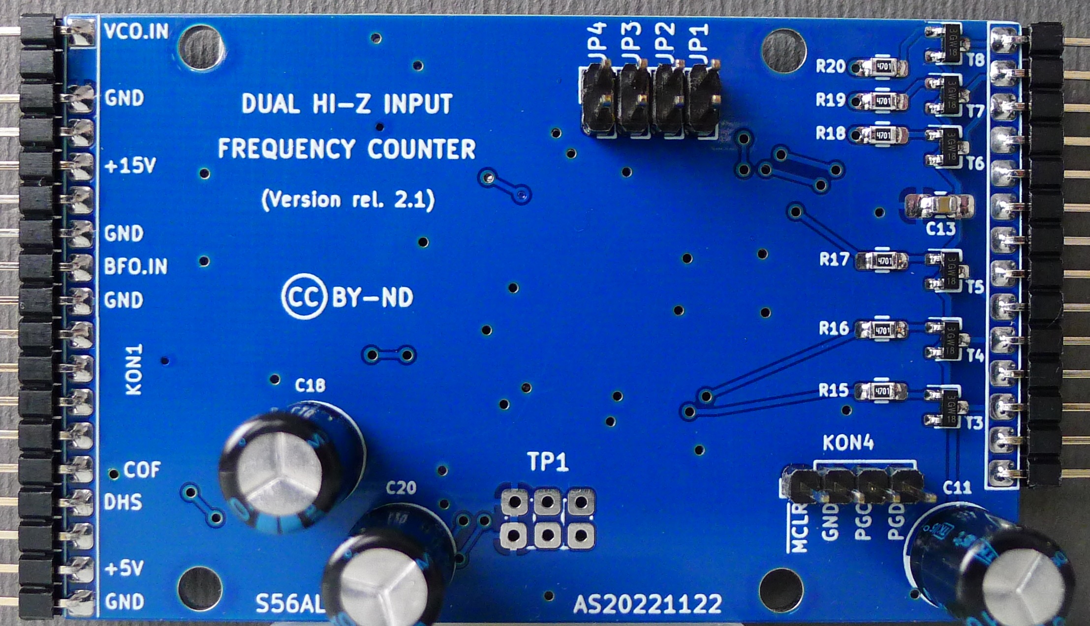
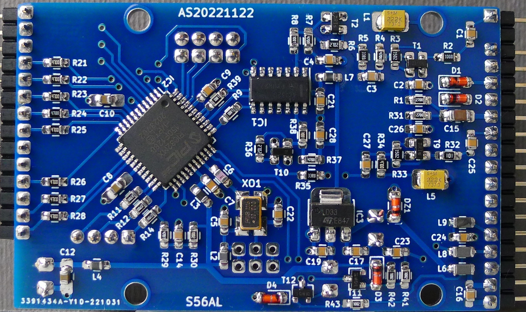
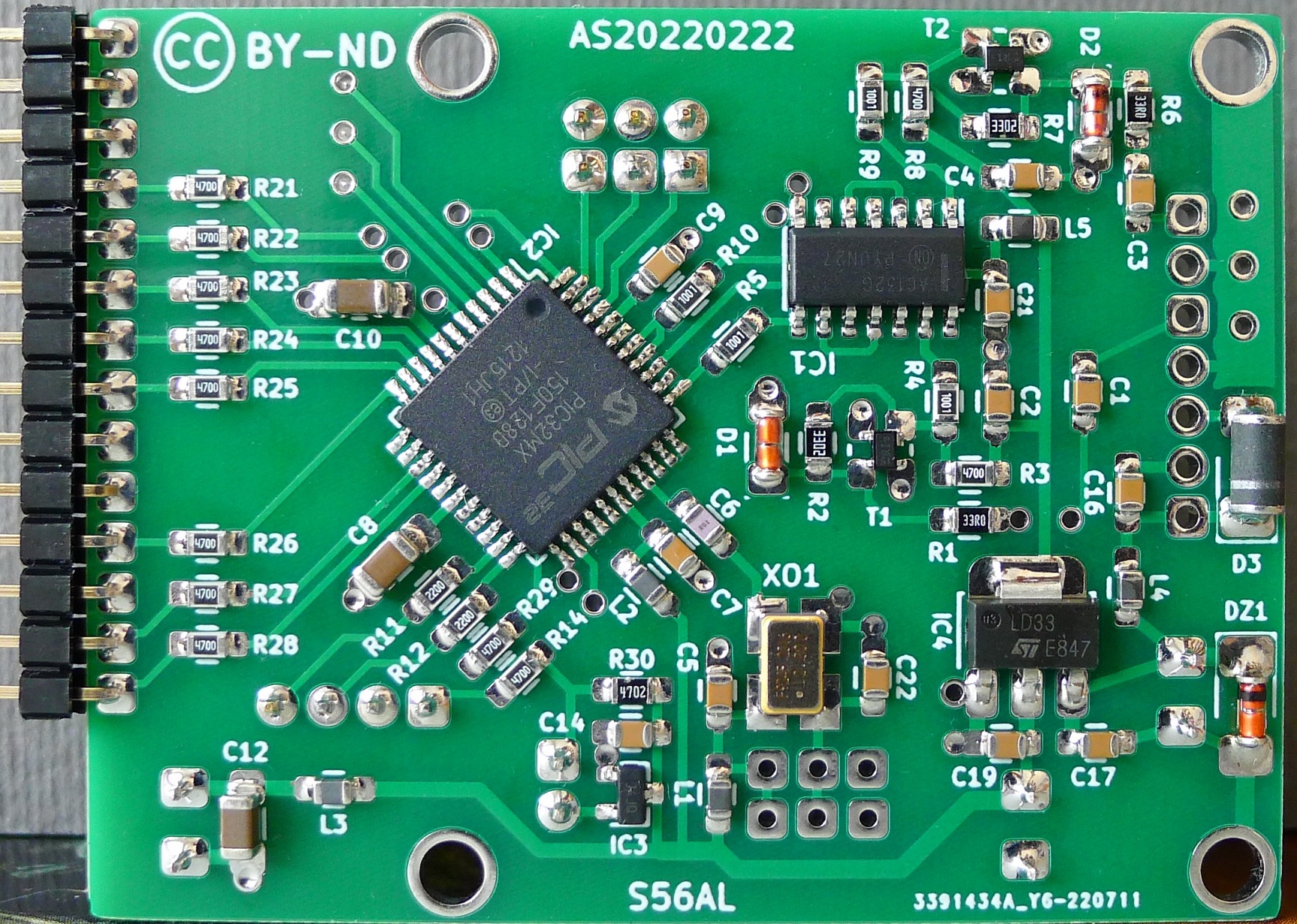
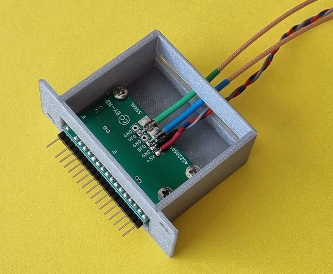
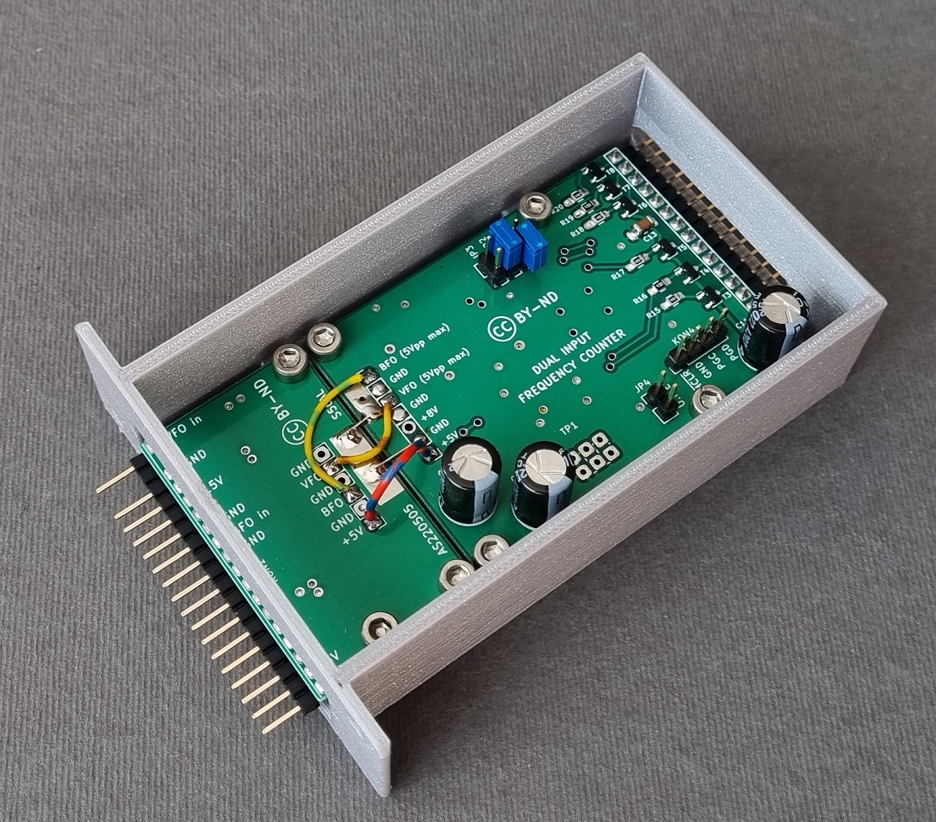
The V2.x release of the TS-820(S) frequency counter design combines the V1.0 main counter board and the separate high impedance input buffer to a single printed circuit board. Additional hardware circuitry and corresponding software functionality has been added to support a traditional as well as a more advanced operating modes:
| a "COG" signal pin interface has been added to the PCB to support the traditional mode of operation; if selected by the jumper the traditional operating mode mimics the original counter behaviour and dims the display in case there is no BFO and/or VFO signal present at the counter frequency signal inputs; | |
| the "DHS" ("display hold function") signal pin interface is now integrated to the V2.x PCB; the presence of an active (logic low) signal at the "DHS" input dims the "MHz" digits in normal operating mode or displays an error message (VFO / BFO input error) in advanced operating mode; | |
| a "traditional operating mode" was added to the firmware (see jumper settings table below). |
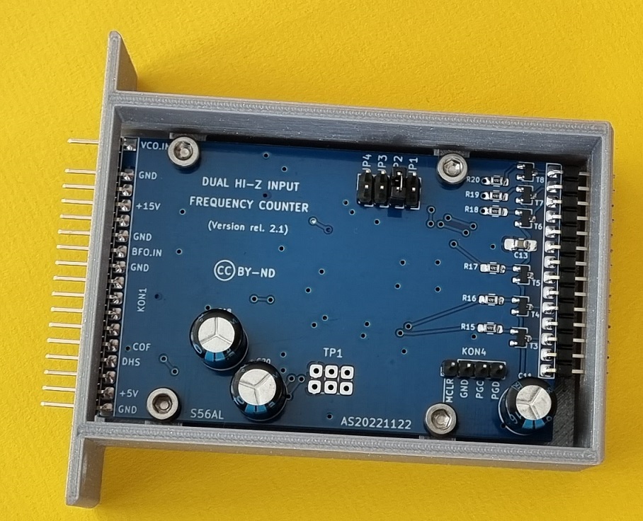
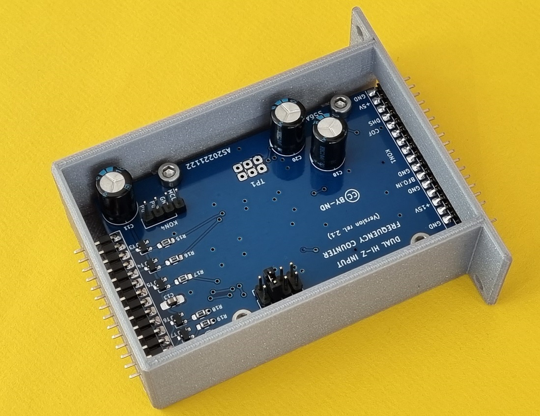
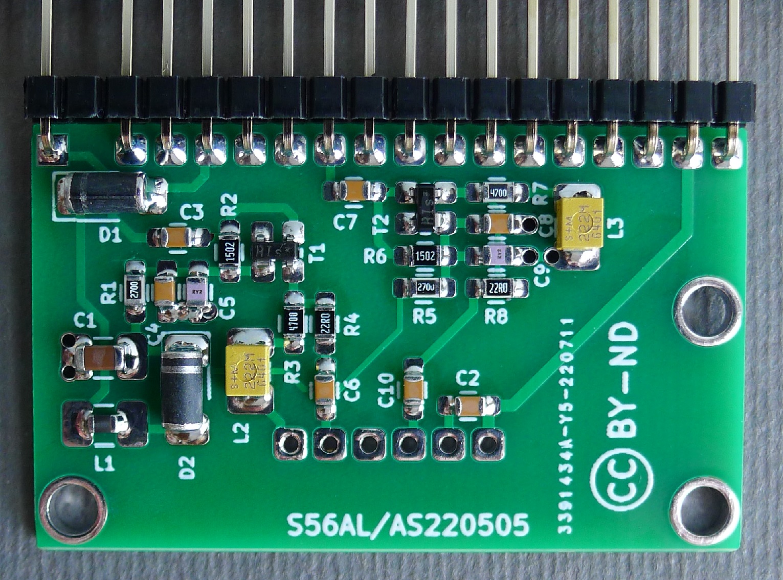
Similar to the release V1.0, the V2.1 integrated counter board is built on a 1,6 mm thick double sided FR4 PCB. The circuit schematics as well as assembly photos of top and bottom side are shown in the pictures below. See the V1.0 main counter board section and the high impedance input buffer description below for further guidance and details.
 |
 |
 |
 |
 |
 |
 |
 |
 |
| PCB layout Ver. 2.1 - Gerber files (96 kB - zip) | PIC32 programming file Ver. 2.1 (hex 5 kB - zip) |
Jumper settings table (Firmware release V2.1)
| JP1 | JP2 | JP3 | JP4 | |
| N.C. | N.C. | - | - | Display intensity: 100% |
| SET | N.C. | - | - | Display intensity: 50% |
| N.C. | SET | - | - | Display intensity: 25% |
| SET | SET | - | - | Display intensity: 12,5% |
| - | - | N.C. | N.C. | Advanced operating mode + hold the display while switching bands |
| - | - | SET | N.C. | Advanced operating mode + dim the display while switching bands |
| - | - | N.C. | SET | Traditional operating mode |
| - | - | SET | SET | Traditional operating mode PLUS |
Version 1.0 - release February, 2022 ... (obsolete, check the V2.x releases above)
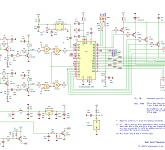
The main counter board circuit schematics as well as assembly photos of top and bottom side of the coresponding PCB are shown in the pictures below. The main counter board is built on a 1,6 mm thick double sided FR4 PCB. Assembly is rather easy, although some skills of SMD soldering are required.
Depending on the LED display units used one may want to adjust the values of the current limiting resistors R21 to R28. With display units purchased from Aliexpress I have found the 330 Ohm resistors to provide more than enough current for clear visibility and sufficient intensity of the frequency displayed. In most cases the brightness has even to be reduced, specially when driving the green LEDisplays. The display brightness can be reduced (adjusted) by jumpers JP1 and JP2 to 1/2, 1/4 or 1/8 of the full brightness. The software supported brightness adjustment is achieved by shortening the time each digit is switched "on" within the 6 digit multiplexing cycle, thus providing some sort of PWM control. The 6 digit LED display multiplexing frequency is 96 kHz (1.0 firmware version), resulting in 16 kHz overall display refrashement rate.
The PIC32MX150 microcontroller firmware has been written in "MikroC PRO for PIC32" / Mikroelektronika development environment.
 |
 |
 |
 |
Jumper settings table (Firmware release V1.0)
| JP1 | JP2 | JP3 | |
| N.C. | N.C. | - | Display intensity: 100% |
| N.C. | SET | - | Display intensity: 50% |
| SET | N.C. | - | Display intensity: 25% |
| SET | SET | - | Display intensity: 12,5% |
| - | - | N.C. | Display hold (DH) function deactivated |
| - | - | SET | DH activated (see the DH switch connection instructions in the text) |
The VFO (VCO) and BFO frequency inputs of the main counter board have been designed as low impedance (50 Ohm). In the main counter board prototypes, built so far, the BFP196 input amplifier transistors (T1, T2) from two different sources has been used. By installing the 33 kOhm feedback resistors (R2, R7), the DC voltage levels between 1,75 and 1,85 V at T1 (T2) collectors have been achieved which should be fine for most applications.
In case one wants to optimise the input sensitivity, a more precise adjustment of R2 (R7) resistance is needed to bring the T1 (T2) collector DC level closer to the targeted 1,65 V. The DC voltage level at T1 (T2) collector can be lowered by soldering additional resistor in parallel to the existing 33 kOhm. 470 kOhm would be a good start. Measure the newely achieved DC level and repeat the process by further lowering the resistance if necessary. 1,65 V is a goal, but there is no need to exaggerate. Anything within +/- 0,1 V should be just fine. The table below shows the measured RF input sensitivity of the main counter board to give an idea how much improvement may be expected / achieved.
| f /MHz | Input sensitivity (@ 50 Ohm) /dBm |
| Optimized Uc (T1) = 1,65 V |
Non-optimized Uc (T1) = 1,85 V |
| 0,1 | - 35 | - 32 |
| 1 | - 34 | - 31 |
| 3 | - 33 | - 30 |
| 10 | - 32 | - 29 |
| 20 | - 29 | - 27 |
| 30 | - 26 | - 24 |
| 40 | - 24 | - 21 |
| 50 | - 22 | - 18 |
| 60 | - 20 | - 15 |
| 70 | - 17 | - 11 |
| 80 | - 14 | - - - |
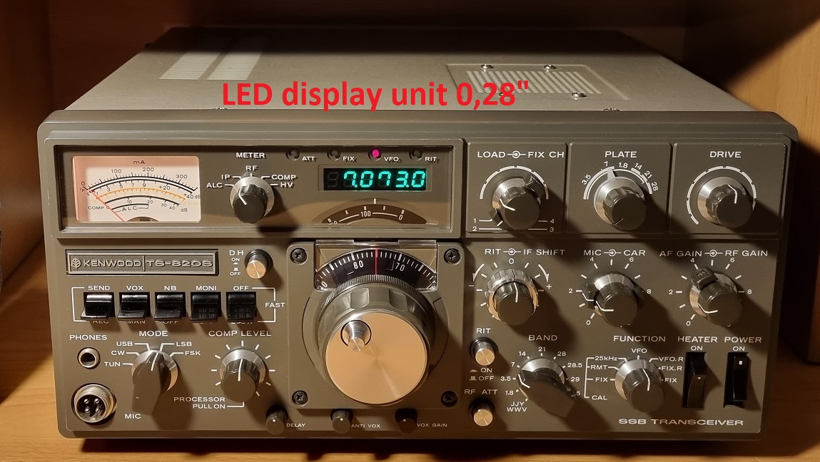
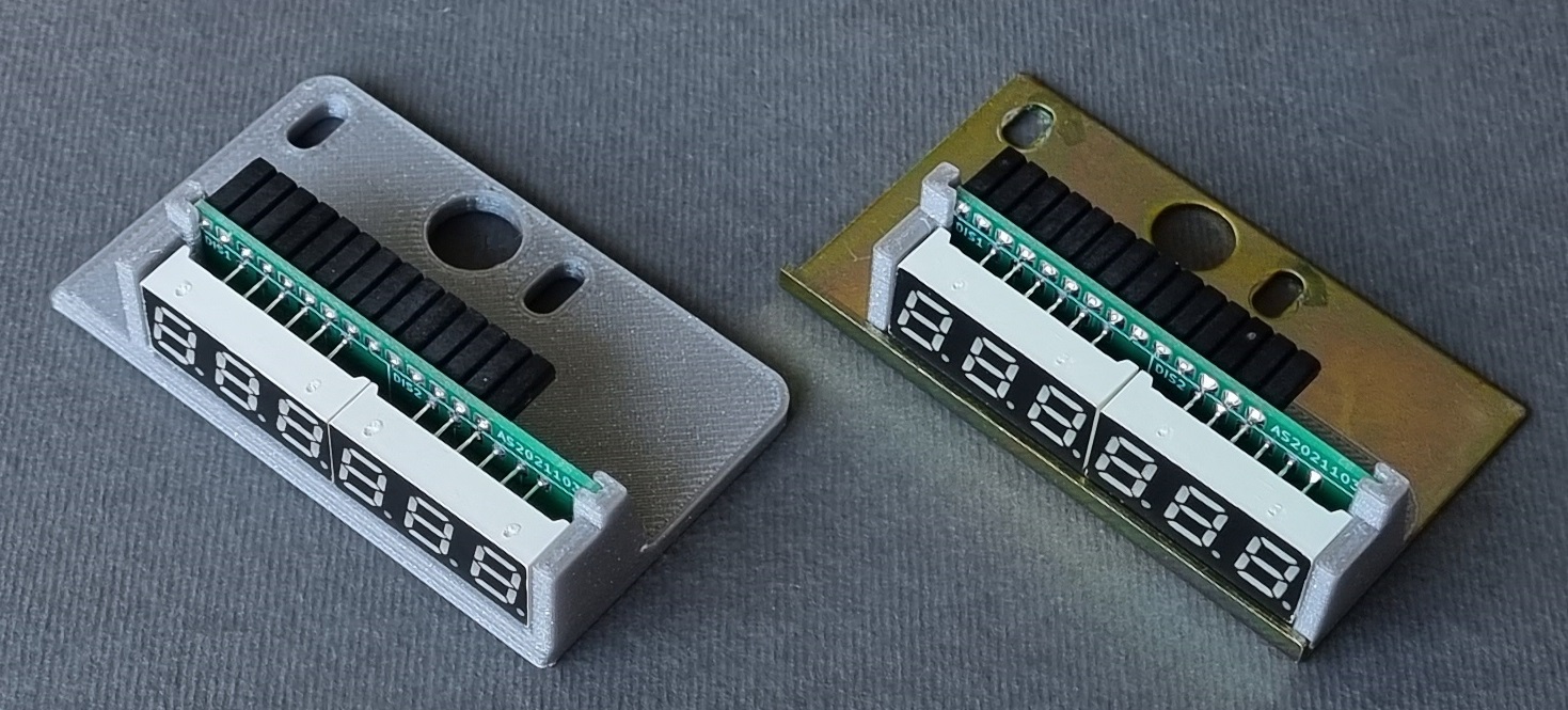
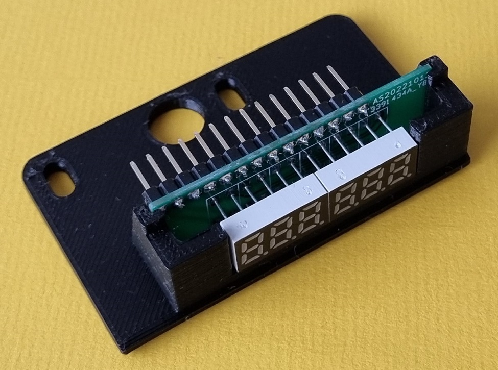
Display unit 0,28"
The 0.28" display unit is built on a 1 mm thick double sided FR4 PCB. Two 3 digit 0,28" 7-segment LED display moduls should be soldered to the board with few milimeters of clearance. Some clearance is necessary, otherwise the display unit will not fit into the TS-820(S). To make the soldering easier a suitable plastic spacer can be 3D printed out of PLA, or better, PETG (see the photo below).
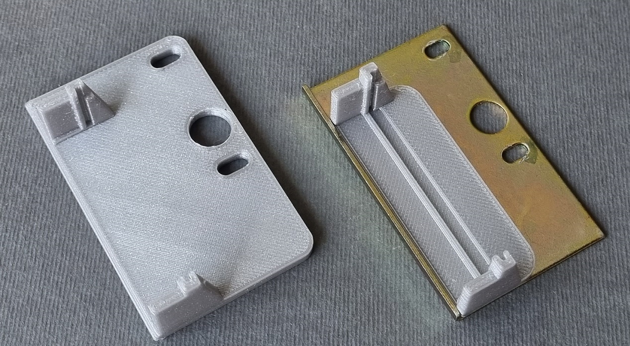
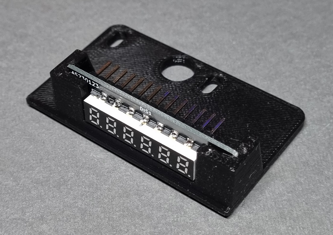
To hold the assembled display unit in place, a plastic bracket was designed and 3D printed in two different layouts/sizes. The smaller bracket is for use with the original TS-820S metal holder (bulb screen). Use double sided "scotch" tape to attach the plastic bracket to the metal base. The larger 3DP display mount allows direct bolting to the TS-820 chassis (see the photos in the "Installation" section). In this case the original metal bulb screen should be removed.
The 0.28" display unit extends practically edge to edge of the transceiver's frequency counter aperture and must be installed very carefully to be visible from a variety of viewing angles (from above as well as straight from the front).
 |
 |
 |
 |
 |
| Display unit 0,28" PCB layout - Gerber files (15 kB - zip) |
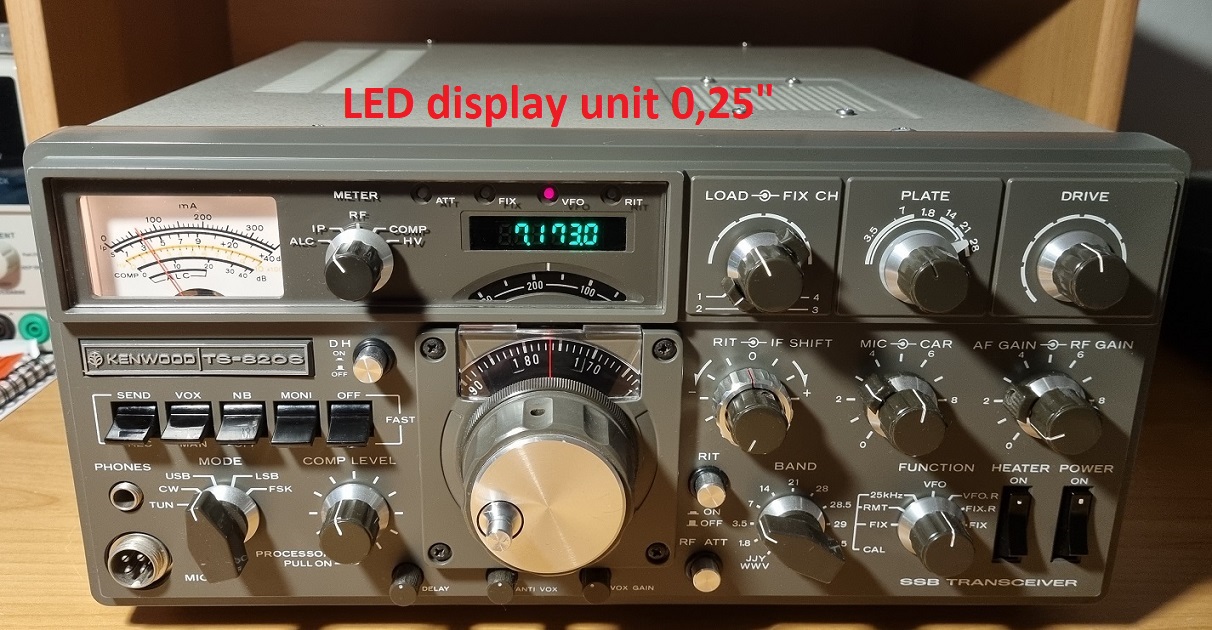
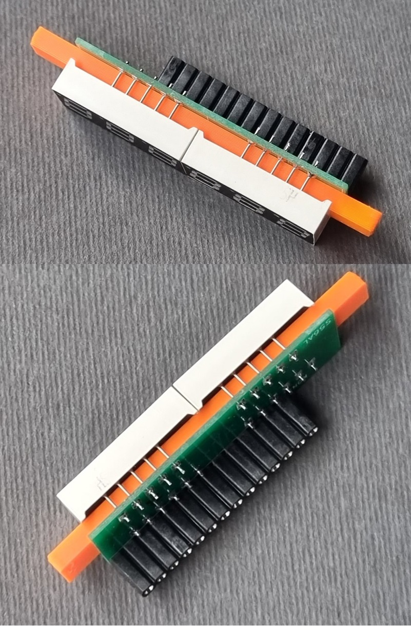
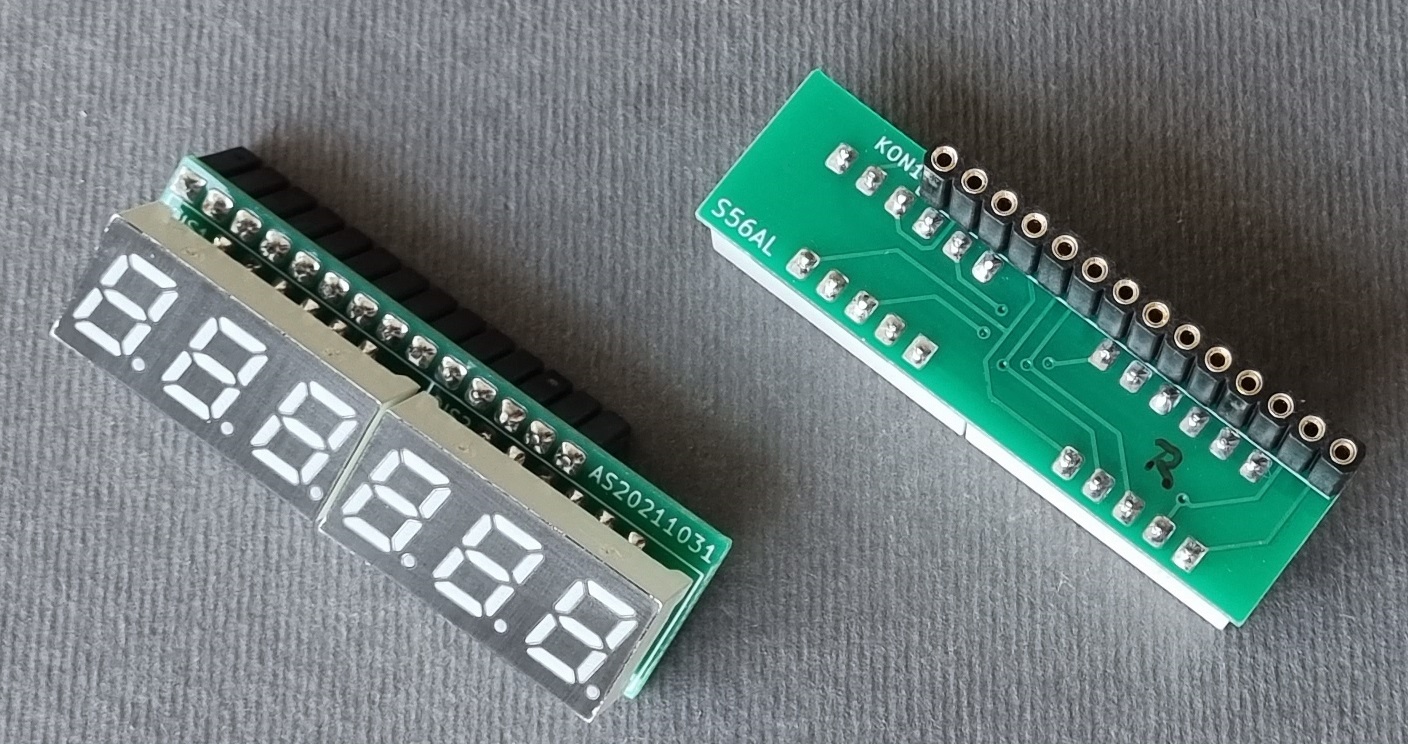
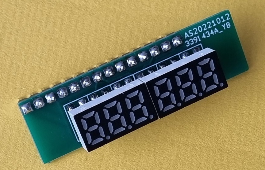
Display unit 0,25"
The 0,25" 7 segment LED display moduls were purchased from Aliexpress. The 3 digit 0,25" modules are available in two versions, with and without the decimal point (DP). The PCB is designed to accommodate LED modules with the DP. The modules without DP have a different pin layout and would not fit the board.
Unfortunately, the 3-digit 0.25" LED display modules are not exactly designed to be placed next to each other in a row (side by side). Therefore, a larger space gap appears between the digits 3 and 4. This can be more or less noticeable when different numbers are displayed (see photos attached).
 |
 |
 |
 |
| Display unit 0,25" PCB layout - Gerber files (10 kB - zip) |
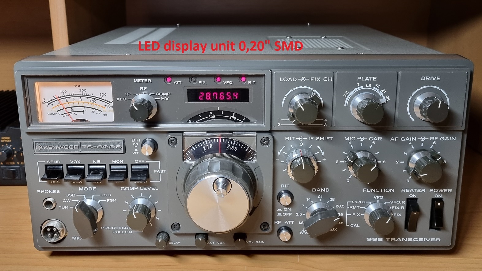
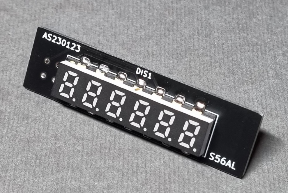
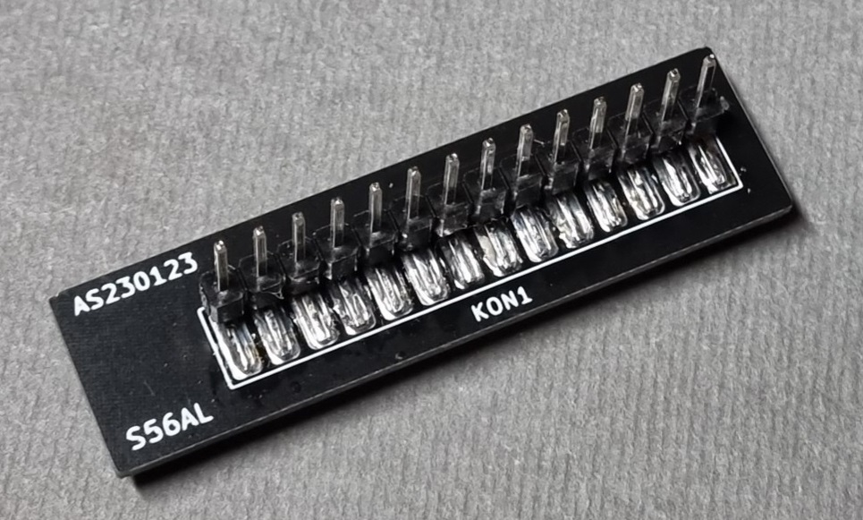
Display unit 0,20" SMD
These 6 digit 0,20" SMD LED display moduls were also purchased from Aliexpress. Many thanks to Juan Carlos WJ6C (ex/CO6BG) for the hint.
The 0,20" size display units seem to be a perfect replacement for the original TS-820(S) displays in terms of size. Unfortunately, I was only able to find them in red colour available (in small quantities) on the market.
 |
 |
 |
 |
 |
| Display unit 0,20 SMD" PCB layout - Gerber files (10 kB - zip) |
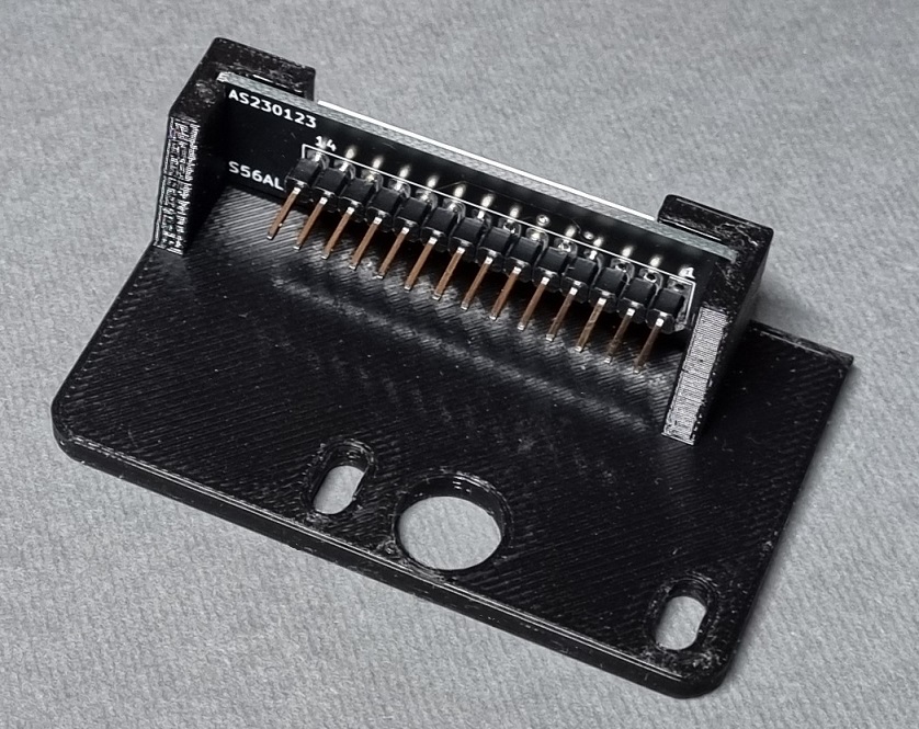
High impedance input buffer (obsolete, check the V2.x counter releases above)
The output impedance of both BFO and VFO (VCO) outputs at the TS-820(S) extension connector is rather high, somewhere around 500 Ohm. Although it is possible to connect the counter's main board low impedance RF inputs to the TS-820 frequency counter extension connector directly, I would strongly advice not to do so. While it would work, it would just not be right. For proper operation the implementation of a simple high input impedance buffer, capable of driving the main counter board's low impedance inputs, as well as isolating them from the transceivers BFO and VFO outputs, is highly recommended.
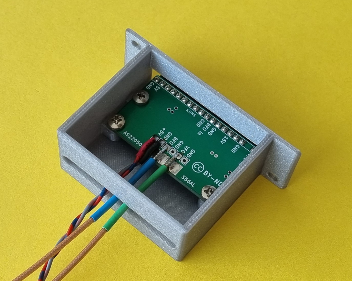
The circuit schematics and assembly photos are shown below. The buffer is built on a 1,6 mm thick double sided FR-4 PCB. Depending on the type of installation (see the "Installation" section), the device can either be installed in to its own bracket or combined together with the frequency counter main circuit board. The STL files for 3D printing of the plastic case (bracket) are attached at the bottom of the page.
 |
 |
 |
 |
| Input buffer PCB layout V1.0 - Gerber files (25 kB - zip) |
Installation I (consider this installation as obsolete)
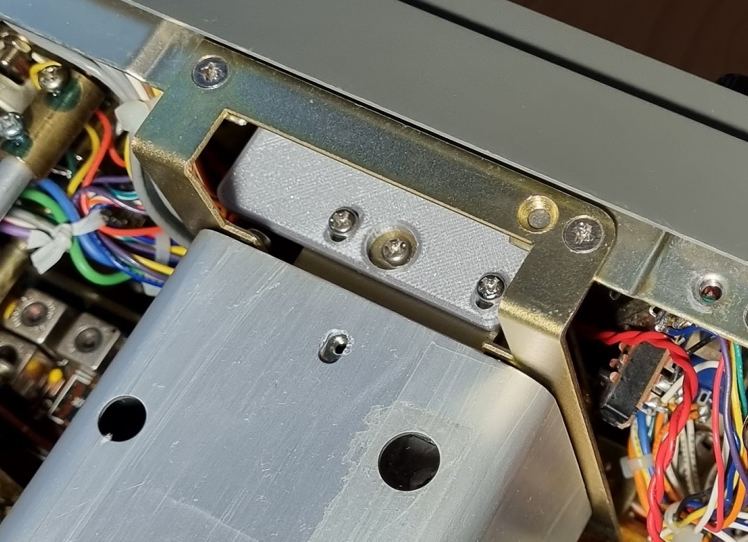
The basic idea was to make installation as easy as possible. That and the intention to keep the connection between the display and main counter unit as short as possible, resulted in the istallation as shown on the photos below. The double sided Scotch tape is used to attach the main counter bracket to the top of the VFO. The doublesided tape is available in different thicknesses, use the thinnest you can get.
Despite the initial assumptions that the connection between the main and display board could be a source of interference, it turned out that the major source of interference is actually the microcontroller itself or more precisely its proximity to the transceiver's bandpass filter board. The interferences are otherwise quite weak, with the antenna connected they are barely noticeable. Some "birdies" may be spoted in the 15 m and 10 m bands, but as already mentioned, only if the antenna is disconnected and the AF volume potentiometer turned way above normal listening level. As soon as the antenna is connected to the transceiver, the birdies, or at least most of them, dive into the HF background noise, picked by the antenna.
 |
 |
 |
 |
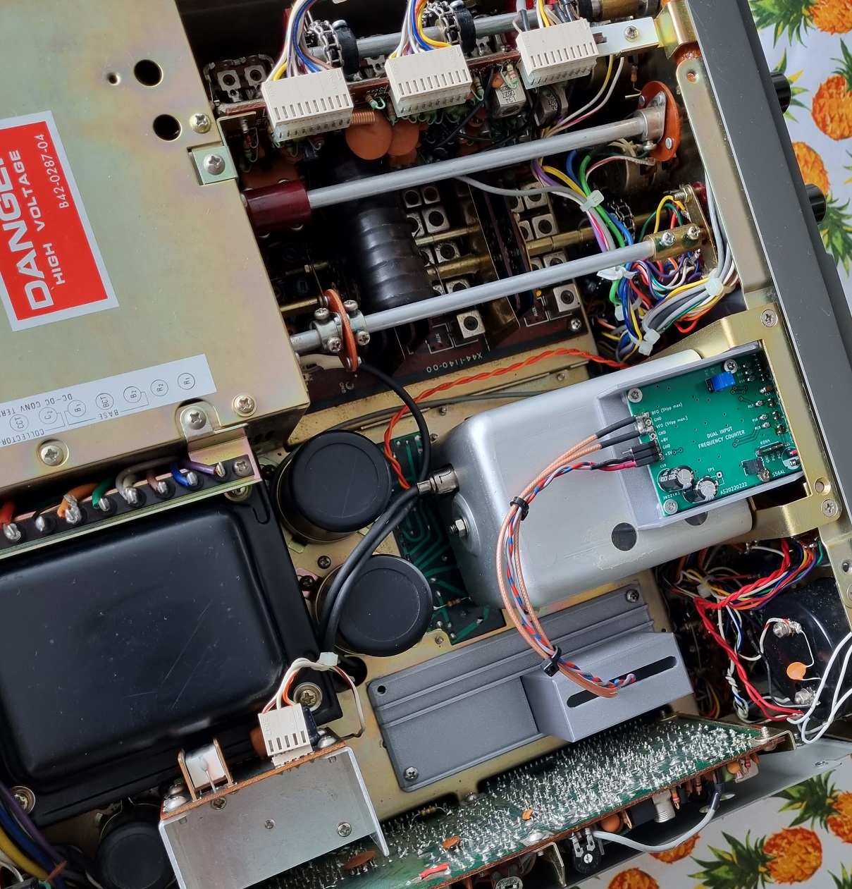 |
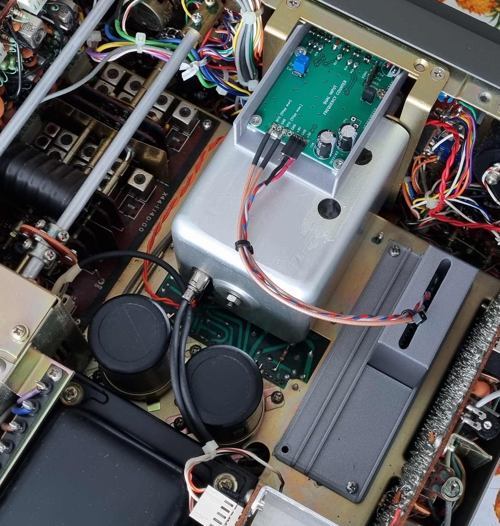
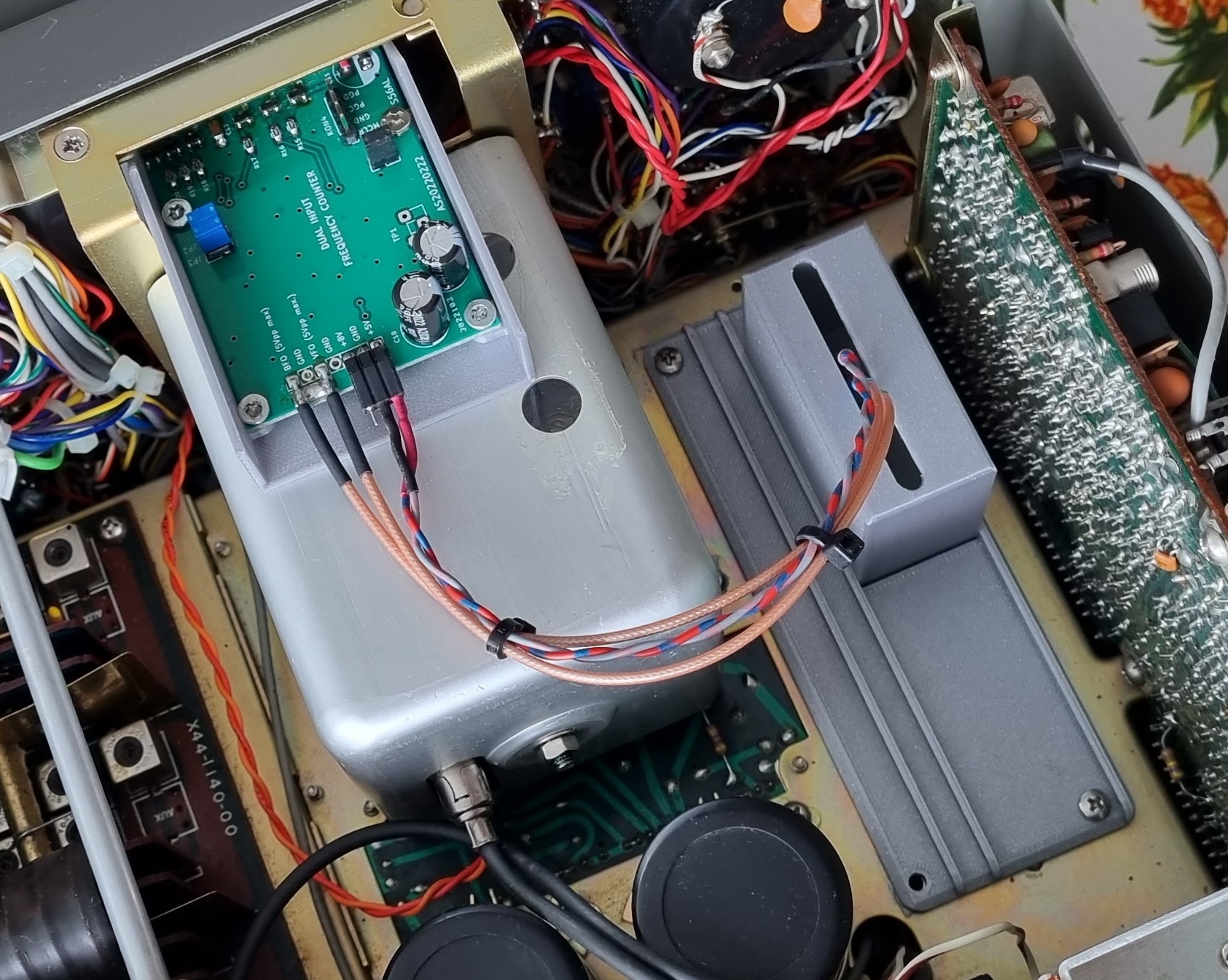
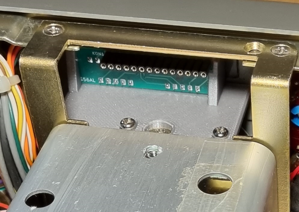
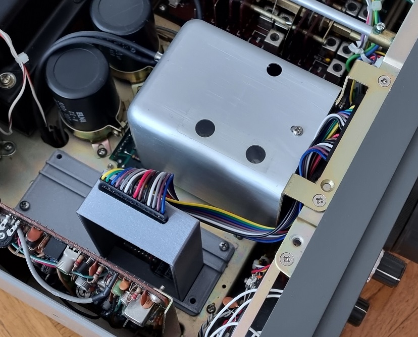
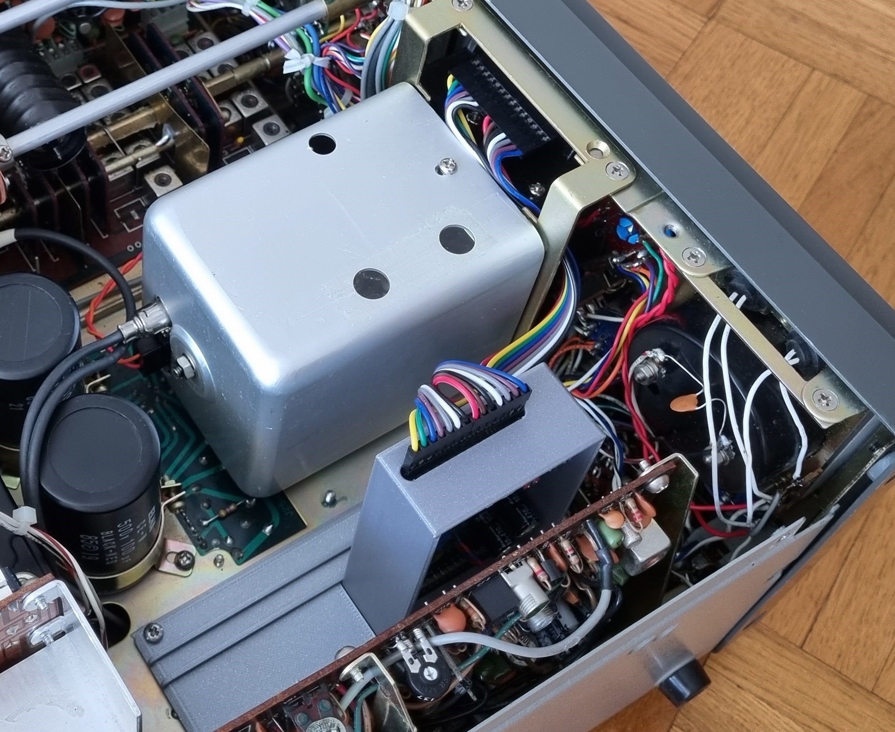
Installation II
Experiments with the replacement frequency counter have shown that the connection between the display and the main board, despite the relatively high multiplexing frequency of 96 kHz and changing nature of the sequence as well as width of the pulses at the display board bus, does not actually cause any internal (local) interference to the transceiver. Considering that and trying to follow the installation concept as originally implemented by the manufacturer, seemed like a better idea. Especially since such an installation results in an increased distance between the counter's microcontroller unit and transceiver's bandpass filter board. The number of unwanted "birdies" has been further reduced and limited mainly to the 10 m frequency band. Again, with a decent antenna connected, the few remaining "birdies" are almost impossible to spot.
 |
 |
 |
 |
 |
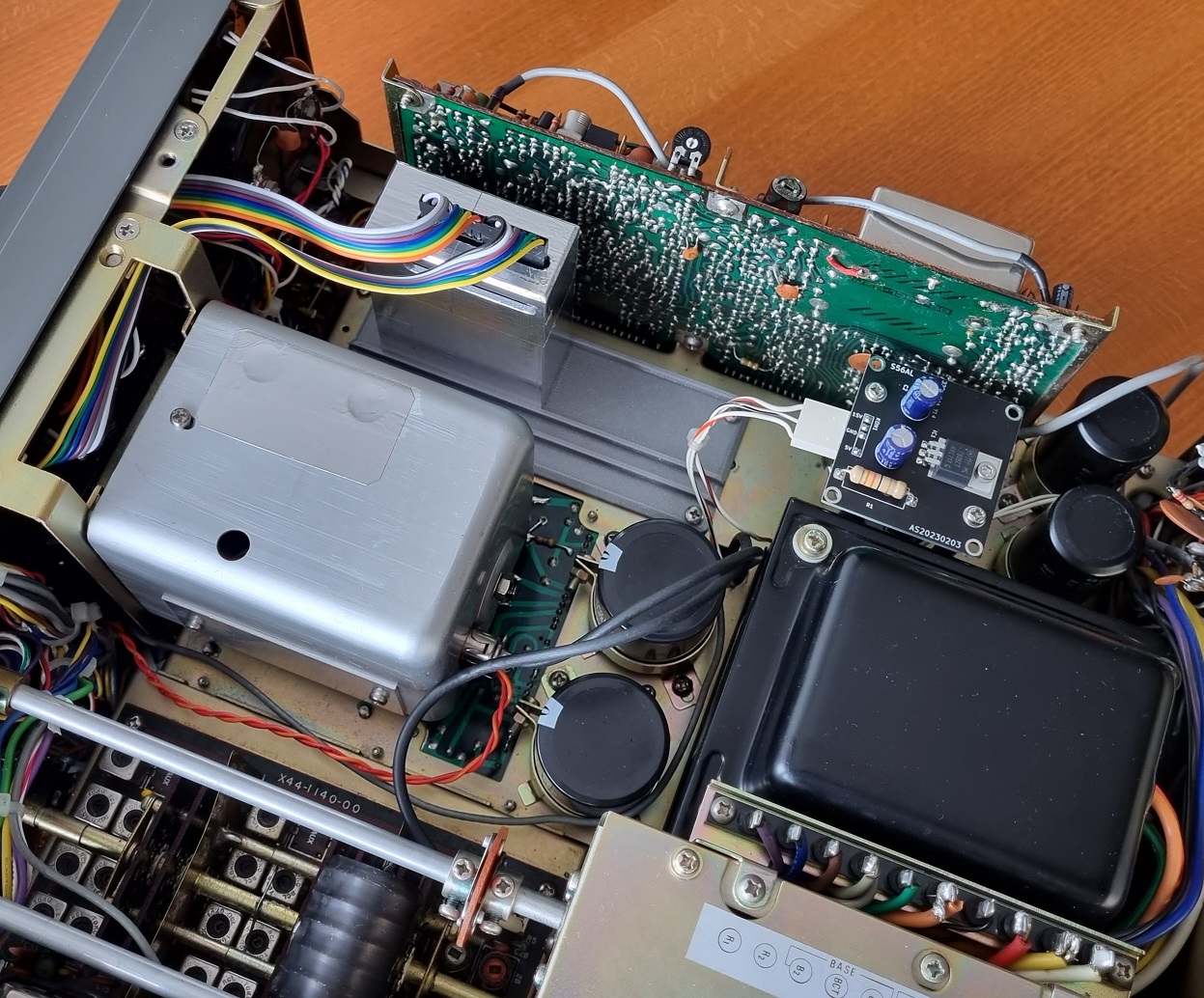
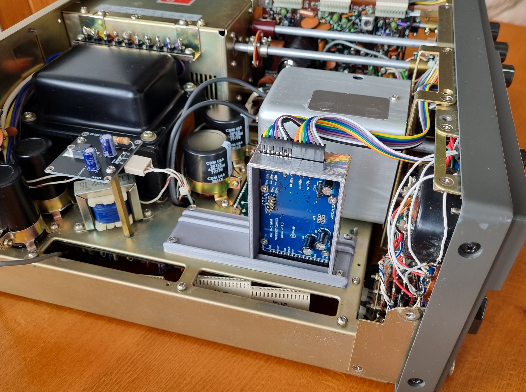
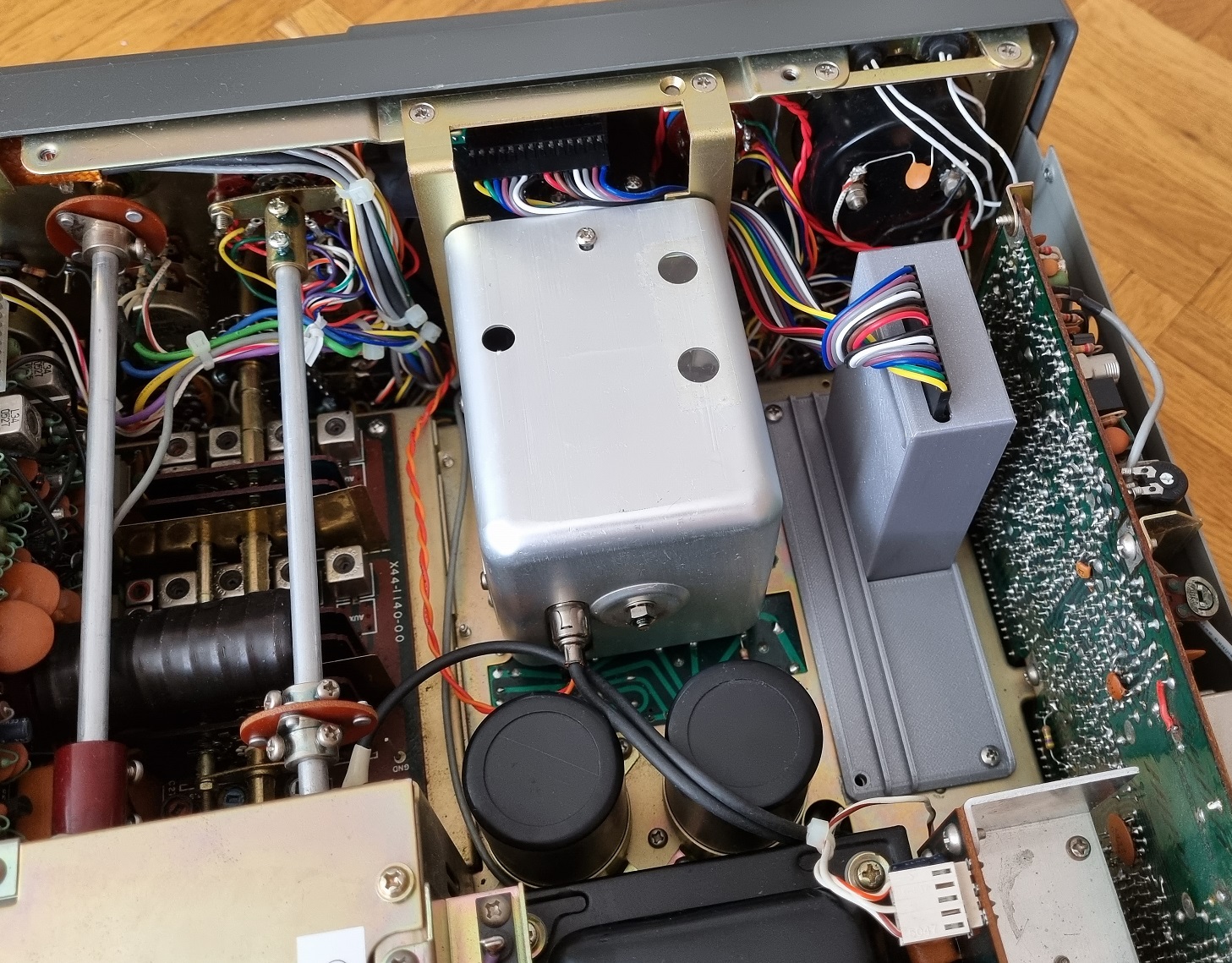
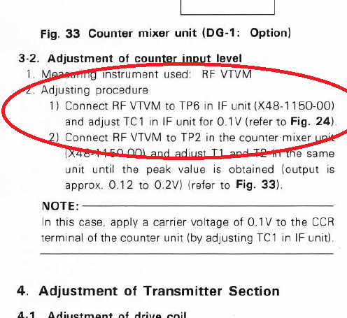
Replacement 5V power supply regulator and the TS-820 (base) model installation particularities
The original frequency counter requires precise adjustment of both input signal levels. The replacement frequency counter is less demanding in this regard. However, when installed in the base TS-820 model, it is still necessary to adjust the BFO level as it seems to be set to the minimum level by the manufacturer.
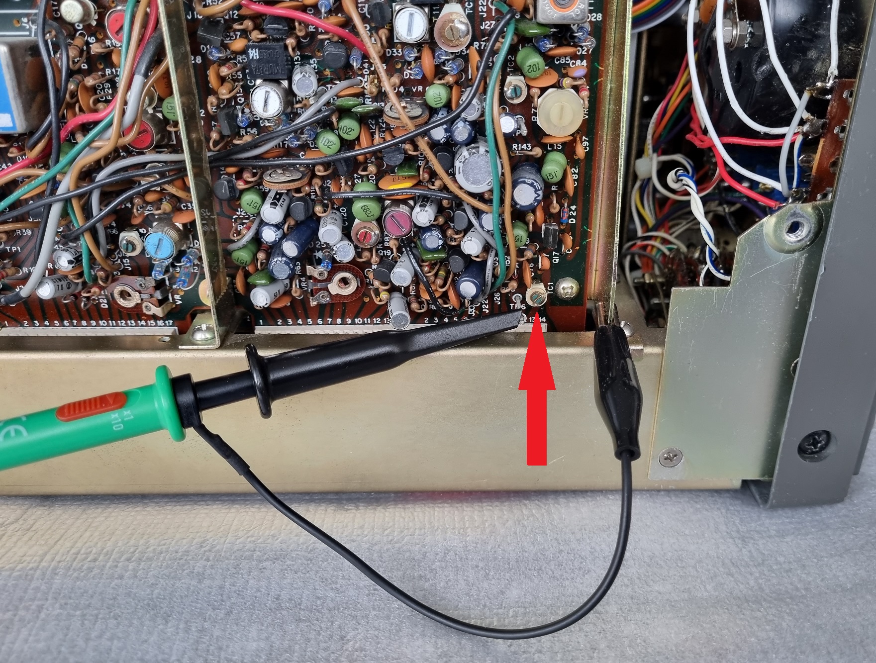
The BFO signal level setup is described in the transceiver's service manual and requires an RF voltmeter with a high-impedance input. In the absence of a suitable measuring instrument, try to ajust the TC1 so that a reliable frequency measurement and a stable frequency display is obtained in both receive and transmit.
 |
 |
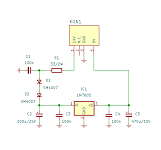
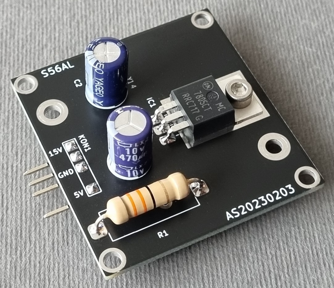
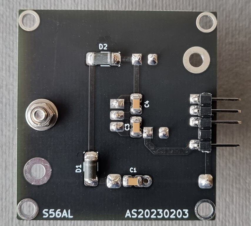
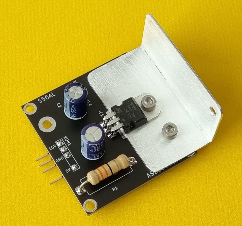
There was no factory installed frequency counter in the base model TS-820 (non "S" version) transceiver. Besides the counter module and coresponding display unit the 15 V to 5 V linear power supply voltage regulator is also missing. To solve this issue a simple replacement voltage regulator was designed. The regulator is built on a double-sided 1,5 mm thick PCB. The current consumption of the replacement counter is drastically reduced compared to the original counter, therefore a simple LM7805 IC voltage regulator can easy handle the necessary voltage drop even without an extra heatsink. Heat dissipation to the PCB as well as through a 33 Ohm resistor is sufficient for the regulator to heat up only moderately.
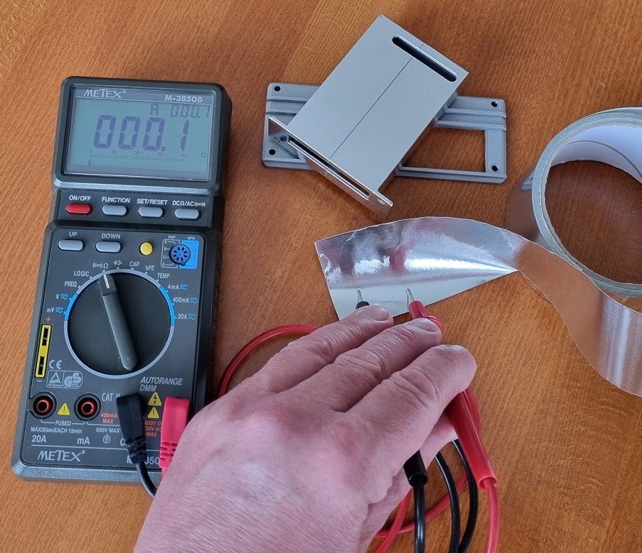
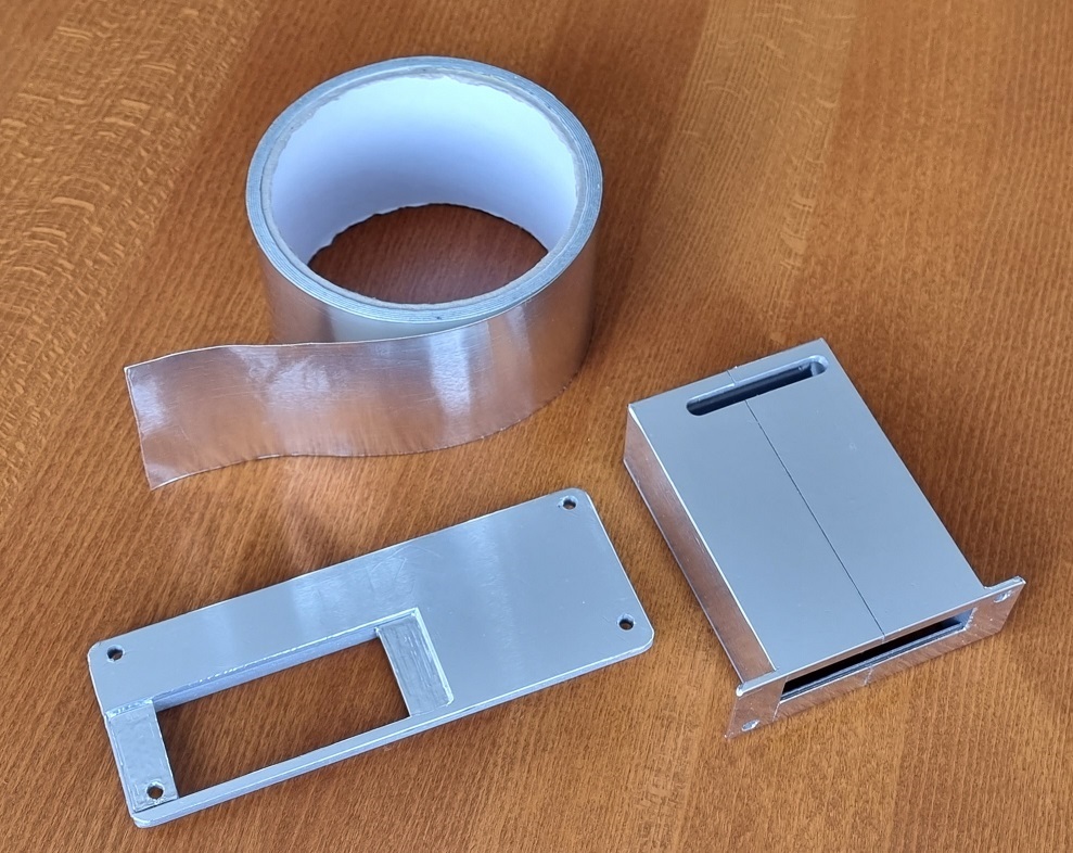
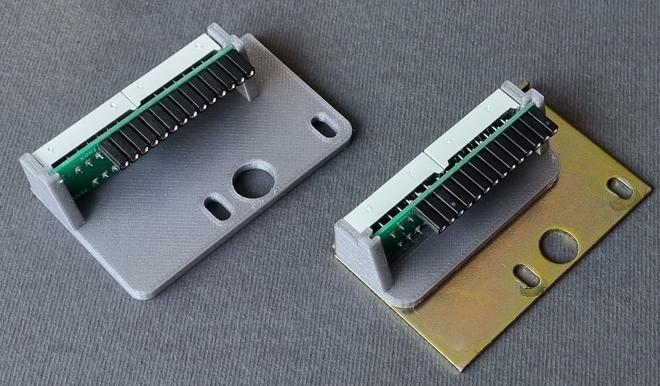
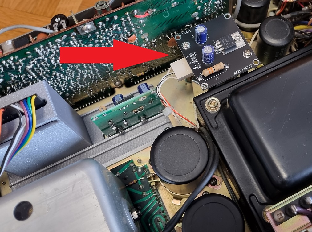
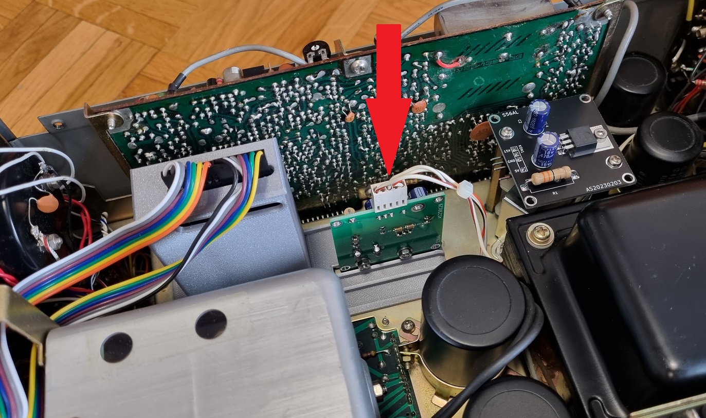
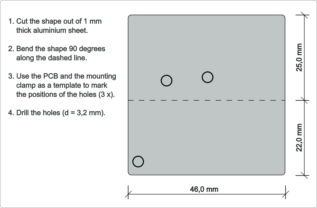
The replacement power supply unit can be installed to the spacers above the power supply choke, as in the case of factory provided solution or it can be placed besides the replacmenet frequency counter and attached by the plastic mounting clamp (see pictures below). The later requires an additional metal mounting bracket cut and bent out of a 1 mm thick aluminium sheet, as suggested in the sketch below.
Please note that the replacement 15 V to 5 V regulator is only designed to power the replacement frequency counter. The replacement voltage regulator cannot power the original Kenwood frequency counter.
 |
 |
 |
 |
 |
 |
 |
| 5V power supply PCB layout - Gerber files (22 kB - zip) |
Plastic parts 3D printing
3D printing of the plastic parts in the PLA should be good enough in most cases. If operation in a higher temperature environment is expected, a more resistant PETG can be used instead.
| Plastic parts - STL files for 3DP (115 kB - zip) | |
| Back to S56AL main page! |
| ...counting since May, 2022. |