| Programmable low jitter FPLL reference clock frequency multiplier
Back to S56AL main page!
|
Release ver. 2.0 (September, 2021)
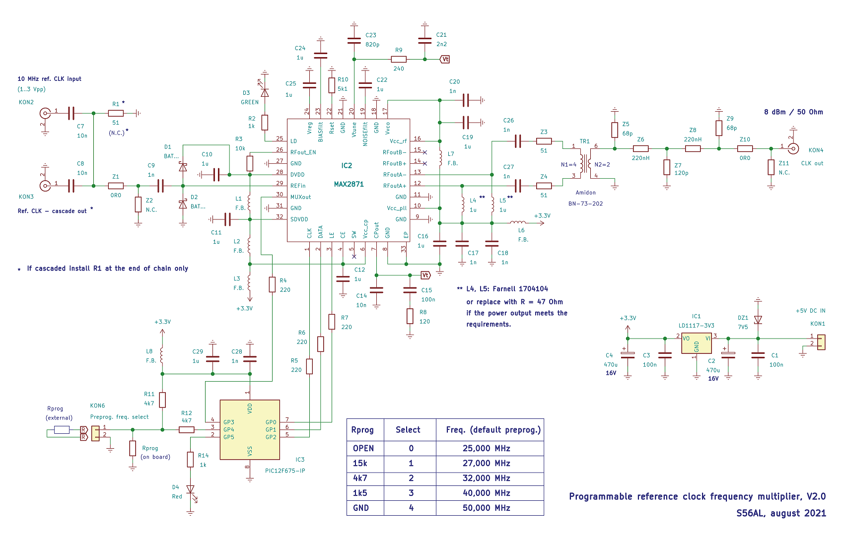
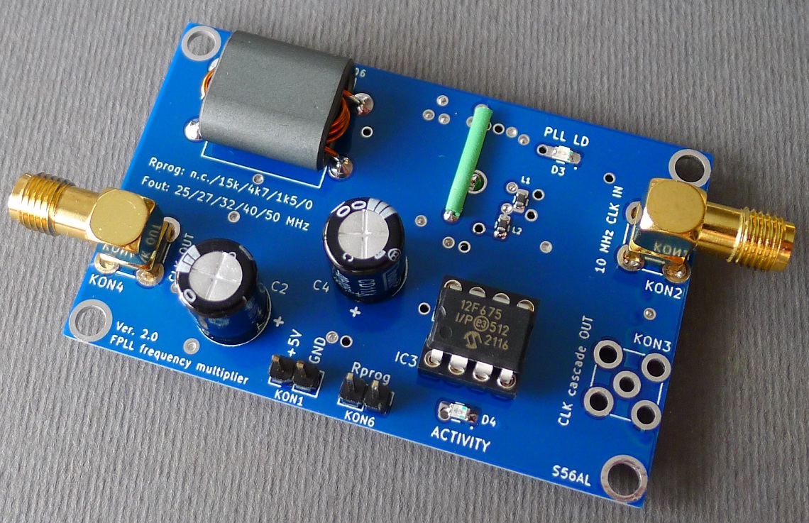
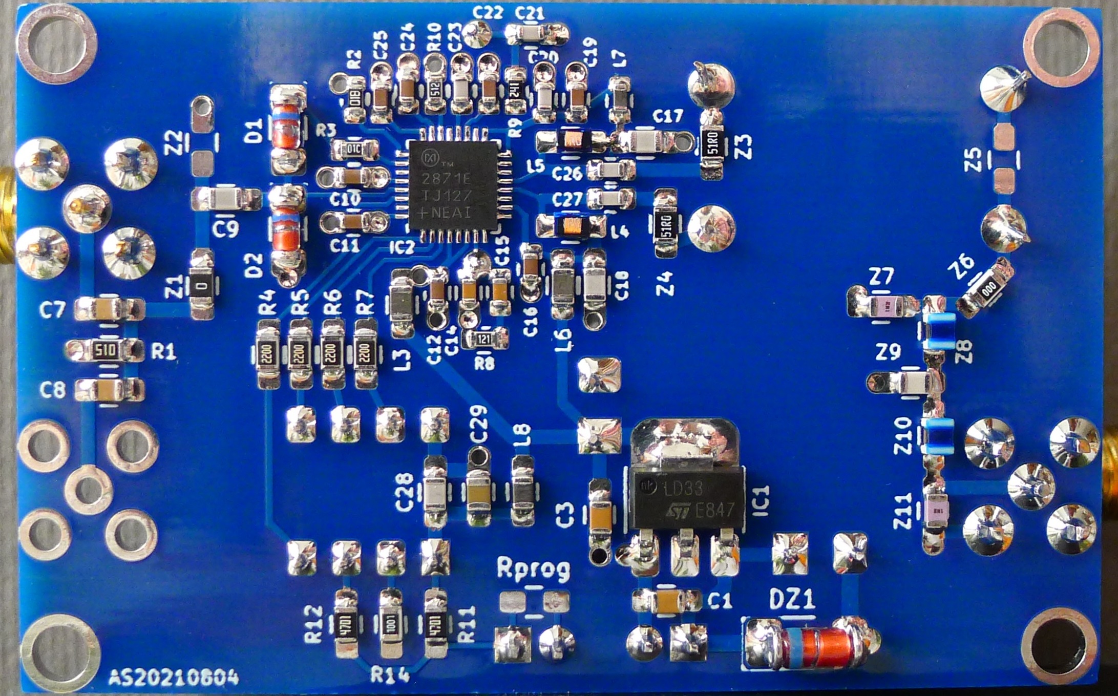
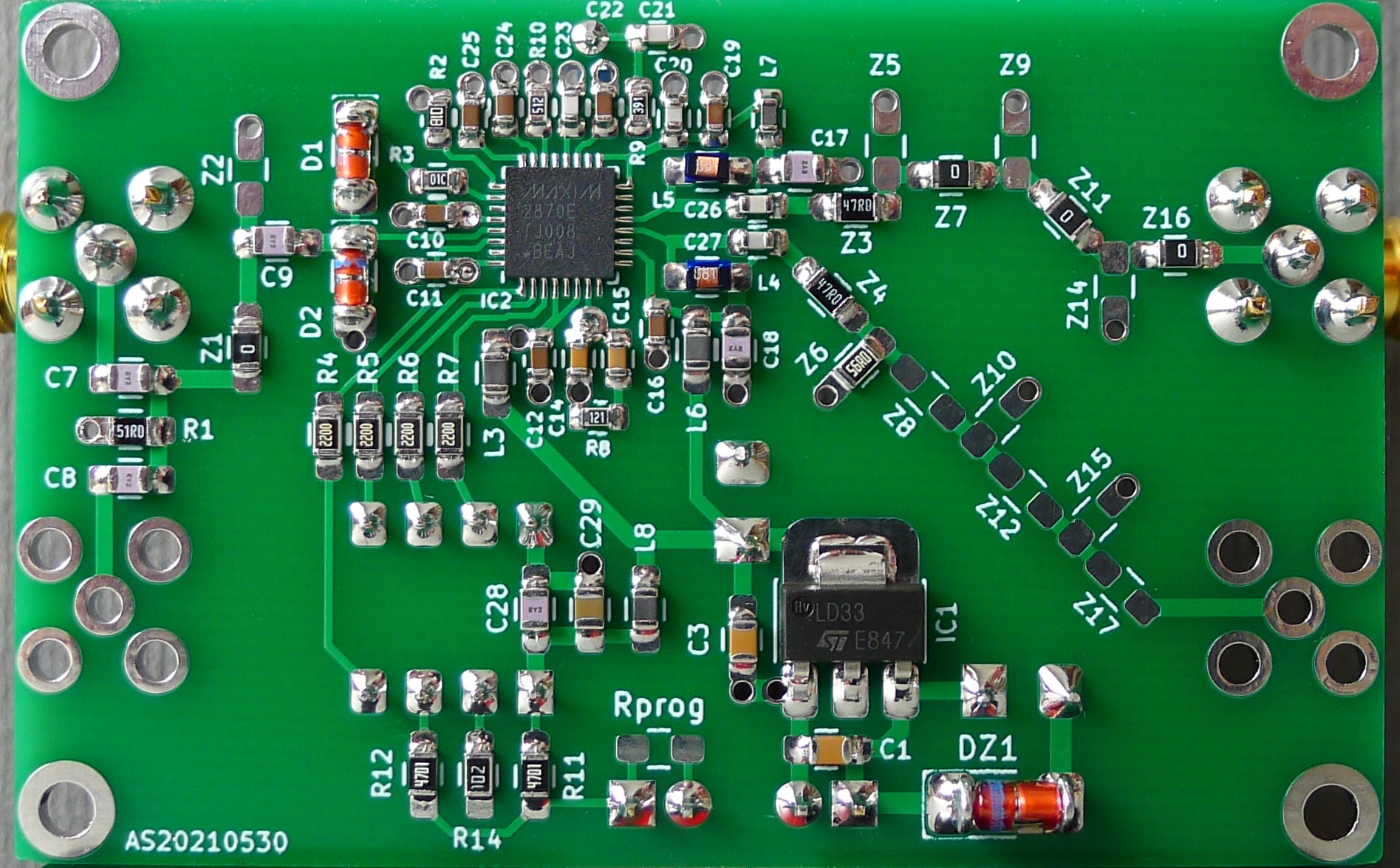
The ver. 2.0 release of the 10 MHz reference clock multiplier introduces a dedicated footprint for a BalUn transformer to the PCB. The BalUn may be wound on a suggested Amidon BN-73-202 or simmilar "binocular" core and ensures a reliable operation in the full output clock frequency range from 25 to 50 MHz. Also the more advanced MAX-2871 has been implemented in the V2.0. The power consumption has slightly increased, in return the phase noise / jitter properties have been improved for a few dB. Nevertheless, there is no obstacle for the MAX-2870 chip to be used on the new version of the PCB as well.
The same PIC12F675 firmware may be used to initialise either of the MAX-2870/2871 chips. However, the more advanced MAX-2871 offers additional settings and further improvement of the phase noise / jitter properties may be achieved by fine adjustments of the FPLL loop tuning parameters, specially the CP-linearity parameter (bits 30:29 of the Register 1) which can be now set to three different values rather than a single one.
|
|
|
| PCB layout / 1,2mm FR4 - Gerber files (183 kB - zip) | |
Release ver. 1.0 (June 2021)
 |
 |
 |
 |
 |
 |
 |
 |
| PIC12F675 assembly source code (4 kB - zip) | PCB layout - Gerber files (195 kB - zip) |
Please note: A certain level of soldering experience as well as basic skills of Microchip's 8 bit PIC family microcontroller programming is necessary to successfully complete the project.
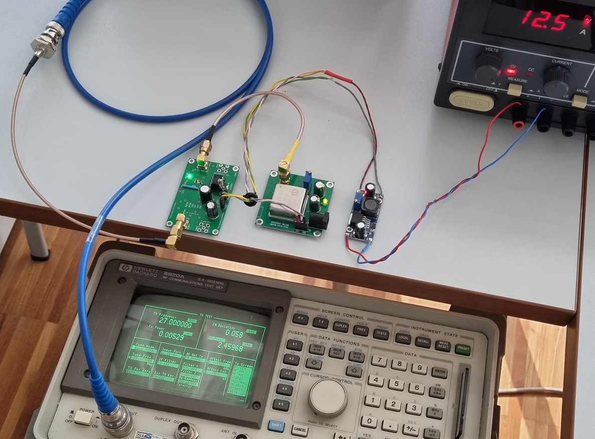
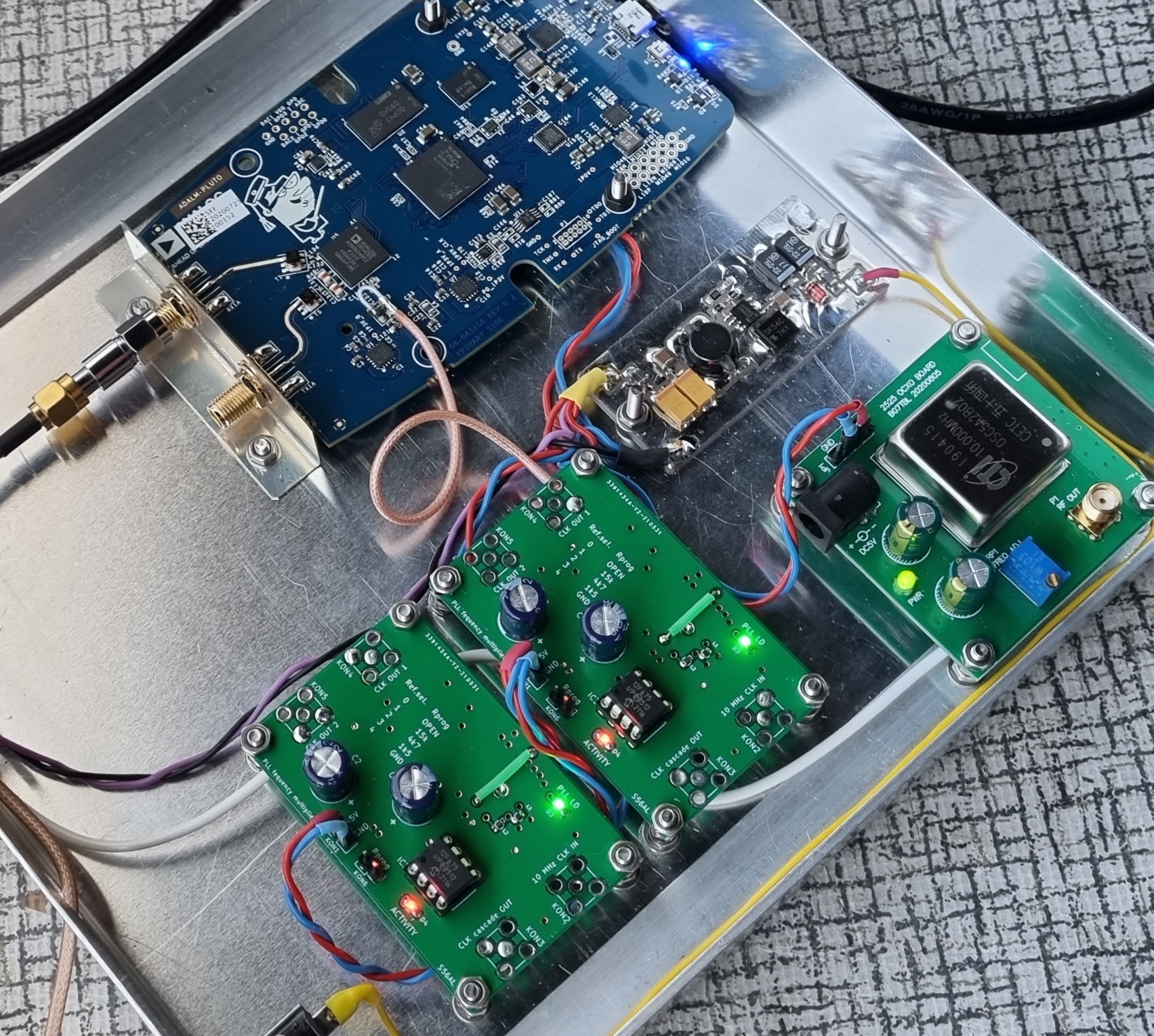
The programmable reference clock frequency multiplier was designed as a solution to provide the necessary reference clock signals for my latest QO-100 RX/TX setup I have been building recently. What I have learned from the previous QO-100 gear setup (built & completed in 2020) was, that for a comfortable SSB voice mode operation it would be highly desirable that all clock signals, supplying the QO-100 transceiver system modules (LNB, TX and RX converters as well as the base station itself) were synchronised from the same (usually 10 MHz) frequency source.
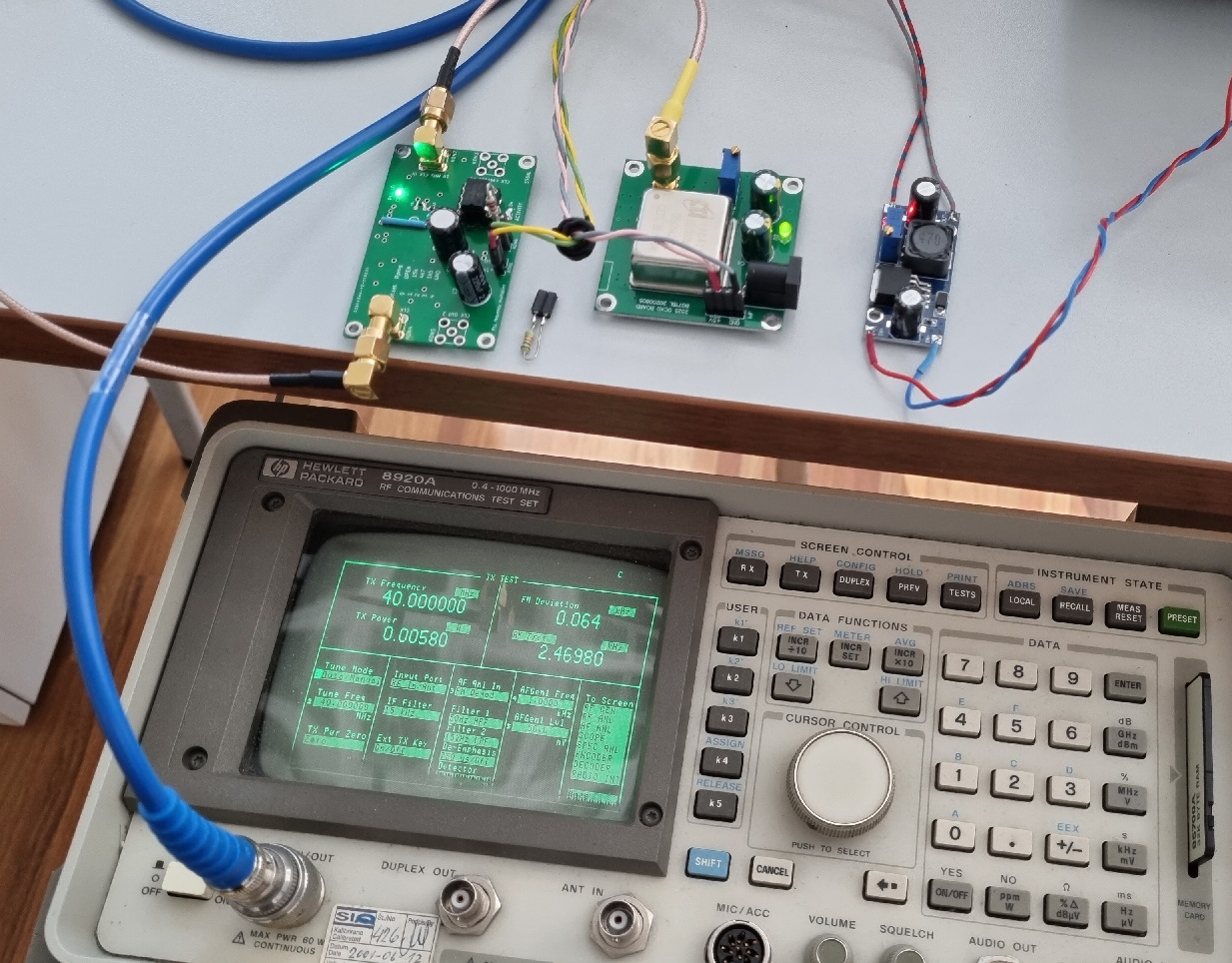
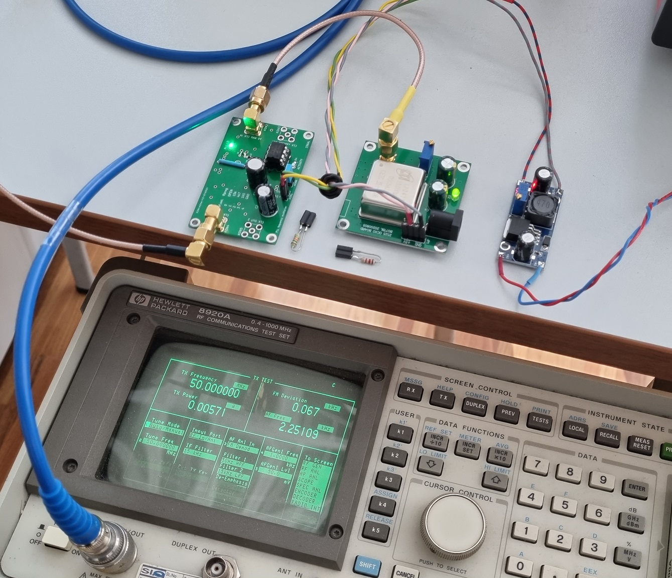
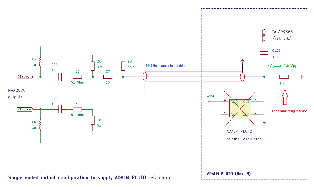
My latest QO-100 transceiver setup is based on an ADLAM-PLUTO configuration and the LNB was modified to accept an external 25 MHz frequency reference source. Thus the frequency reference clock signals of 25 and 40 MHz are to be generated from a common 10 MHz source. Although the ADALM-PLUTO system is flexible regarding its reference clock and may be reprogrammed to values different from the factory default 40 MHz, some issues have been reported by people trying to feed the PLUTO from a 10 MHz reference frequency clock source directly.
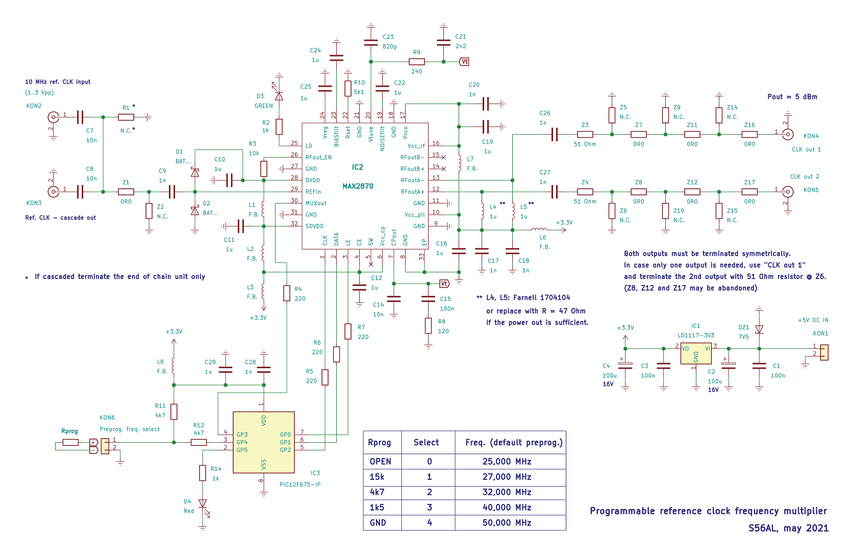
The frequency multiplier circuit is based on a well known MAX-2870 single chip FPLL. The IC is available in a 32 pin TQFN housing (with additional GND exposed pad at the bottom of the case) and is able to provide a huge range of possible frequencies down to 23 MHz. The jitter / phase noise of the generated output signal as specified by the manufacturer should be good enough for the purpose.
The whole design was highly inspired by a frequency synthesizer used in the 10 Mbps BPSK ZIF amateur packet radio transceiver (1.2 to 3.4 GHz) designed by Matjaz S53MV. I have directly copied the cleverly designed controller part based on a Microchip's 8 bit PIC12F675 device. Only a few minor modifications have been necessary to adjust the original assembly program, written by Matjaz, to perform the new task.
Apart from the necessary adjustments of the values, programmed into the MAX-2870 register-set to obtain the desired output frequencies, a couple of assembly lines have also been added to support the "Activity/Status" LED signalling. As Matjaz is well known for his ascetic way of programming, one can easily distinguish the originally written program lines from those added afterwards. Also the assembly language mnemonics added by myself are being written in lowercase rather than capital letters.
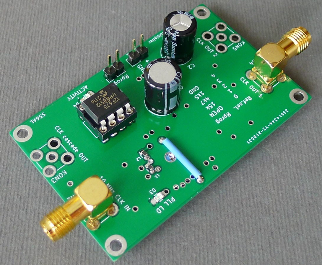
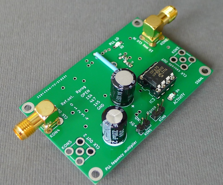
Five frequencies are preprogrammed into the multiplier by default and can be selected by attaching a corresponding resistor (Rprog) to the KON6 header (see the table below). There is also a footprint for a programming resistor provided at the PCB bottom side (Rprog, SMD 0805) for a more permanent output frequency selection.
Selection of the preprogrammed output clock frequency
| CLK out frequency (default preprog.) | Rprog value | |
| 1. | 25,000 MHz | OPEN |
| 2. | 27,000 MHz | 15 kOhm |
| 3. | 32,000 MHz | 4,7 kOhm |
| 4. | 40,000 MHz | 1,5 kOhm |
| 5. | 50,000 MHz | GND |
Some degree of flexibility regarding the input (10 MHz) as well as output clock signal levels has been achieved by additional footprints available on the PCB (compnents marked as "Z" in the schematics) to either adjust the signal levels by capacitive/resistive dividers or to filter the output clock signal if convenient so. For example, to get a more clean sine output. Although the latter would rarely be necessary in real world applications. Furthermore, some devices (like PLL chips) are even "happier" if fed by a square wave reference clock signals rather than a pure sine.
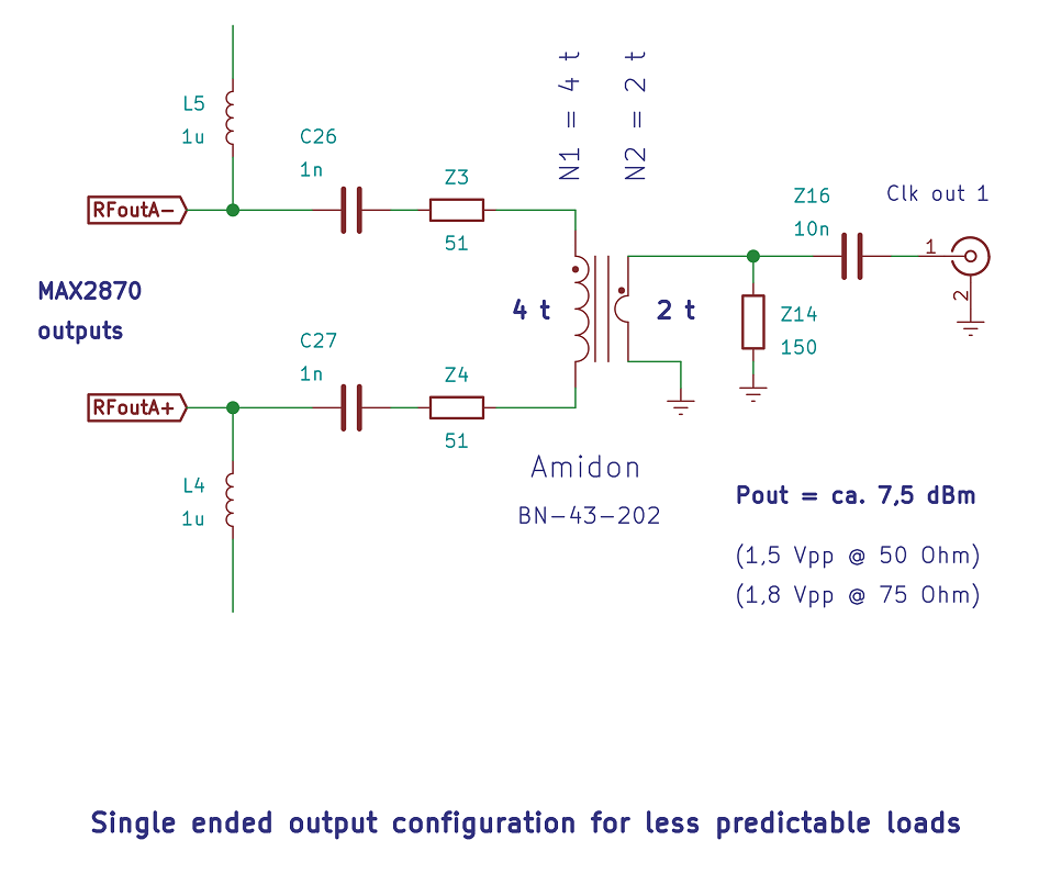
It is also very important to keep in mind that both MAX-2870 outputs must be terminated equally / symmetrically for the output stage to work properly and provide the amount of output power specified by the manufacturer.
In case only one output is needed (this would be most of the cases, I guess) and the load impedance of the device fed by the clock output is well defined, the 2nd output can simply be terminated in the corresponding impedance.
When the load impedance is not so well defined, it is highly recommended to use a sort of a balancing circuitry (BalUn) that will take care of terminating both MAX-2870 outputs equally. A simple transformer wound on a binocular ferrite core (like Amidon BN-73-202 or BN-43-202) will serve the purpose just fine for the whole frequency range of 25 to 50 MHz.
(CLICK the drawing TO MAGNIFY)
 |
 |
The multiplier is built on an 1,2 mm thick FR4 PCB. Keep that in mind if you decide to order the PCBs from a manufacturer. The rest is more or less obvious from the circuit schematics and assembly photos, not much more to say about it.
| Back to S56AL main page! |