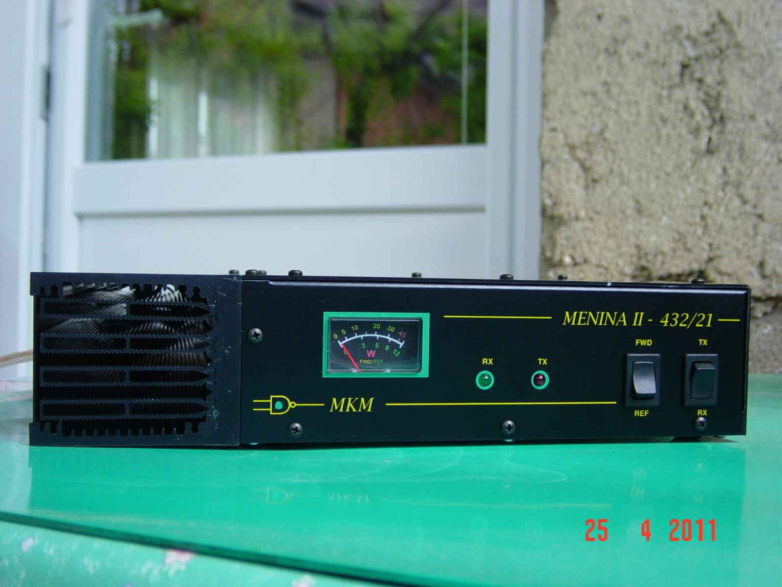
Menina II 432/21 MHz transverter
After success on 144 MHz
with Javornik 144/14 transverter,
Franci - S51RM, Robi –
S53WW and me decided to build transverter for 432 MHz. We use parts of electrical and complete mechanical
design from Javornik II transverter.
Major changes are in oscillator (411 MHz) compartment. There is 137 MHz XTAL
and multiplier (x3). We redesigned IF to 21MHz. Directional coupler and output
LP filter was recalculated. RX chain was designed for two stage amplifier for
both synchronous receivers. First stage is preamplifier at the antenna with
ATF-54143 (slightly modified YU1AW design with built
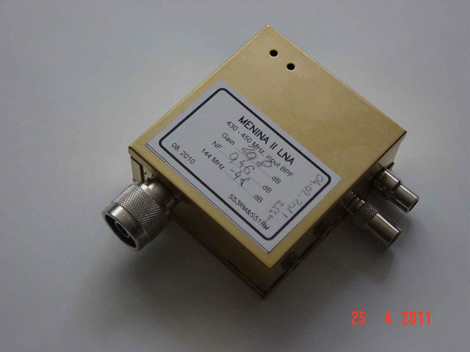
in input band pass filter and notch filter for 144 MHz - G=20 dB, NF=0.5 dB)
and high input IP3 amplifier in Menina II transverter with SGA-6389. For stand-alone operation with transverter,
there is built in preamplifier (only for main RX and antenna connected to ANT
432 MHz) with HMC-374.
RX input band pass filter
in Menina is 10 MHz (-3dB) wide. With general
coverage HF transceiver (19 - 29 MHz) one can easily cover 430 – 440 MHz band.
TX filtering is a bit narrower. (8 MHz at -3dB).
Both preamplifiers with
antenna relays included can be feed through central wire of RX coaxial cable.
13V / 500mA is available at ANT1 IN and ANT2 IN BNC
connectors through jumper inside Menina II. Transverter is short circuit protected with polyswitch resettable device on board. If you operate that
way, TX and RX chain must be separated at the antenna coaxial relay and driven
to power amplifier and ANT1&2 IN (RX inputs of Menina
II) separately. All the TX/RX sequencing is done by Menina
II transverter, so there is no need for external
separate sequencer in order to properly switch power amplifier(s) and
preamplifiers.
|
|
Menina II
front view. |
|
|
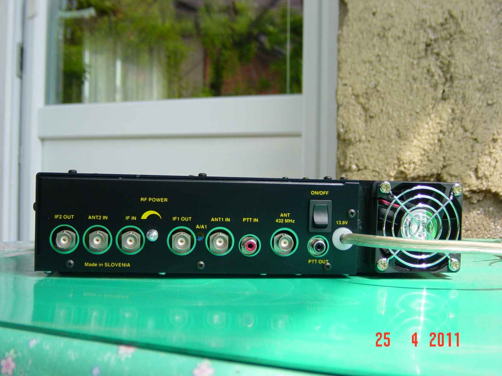
Menina II
back view. |
|
|
|
|
|
|
|
|
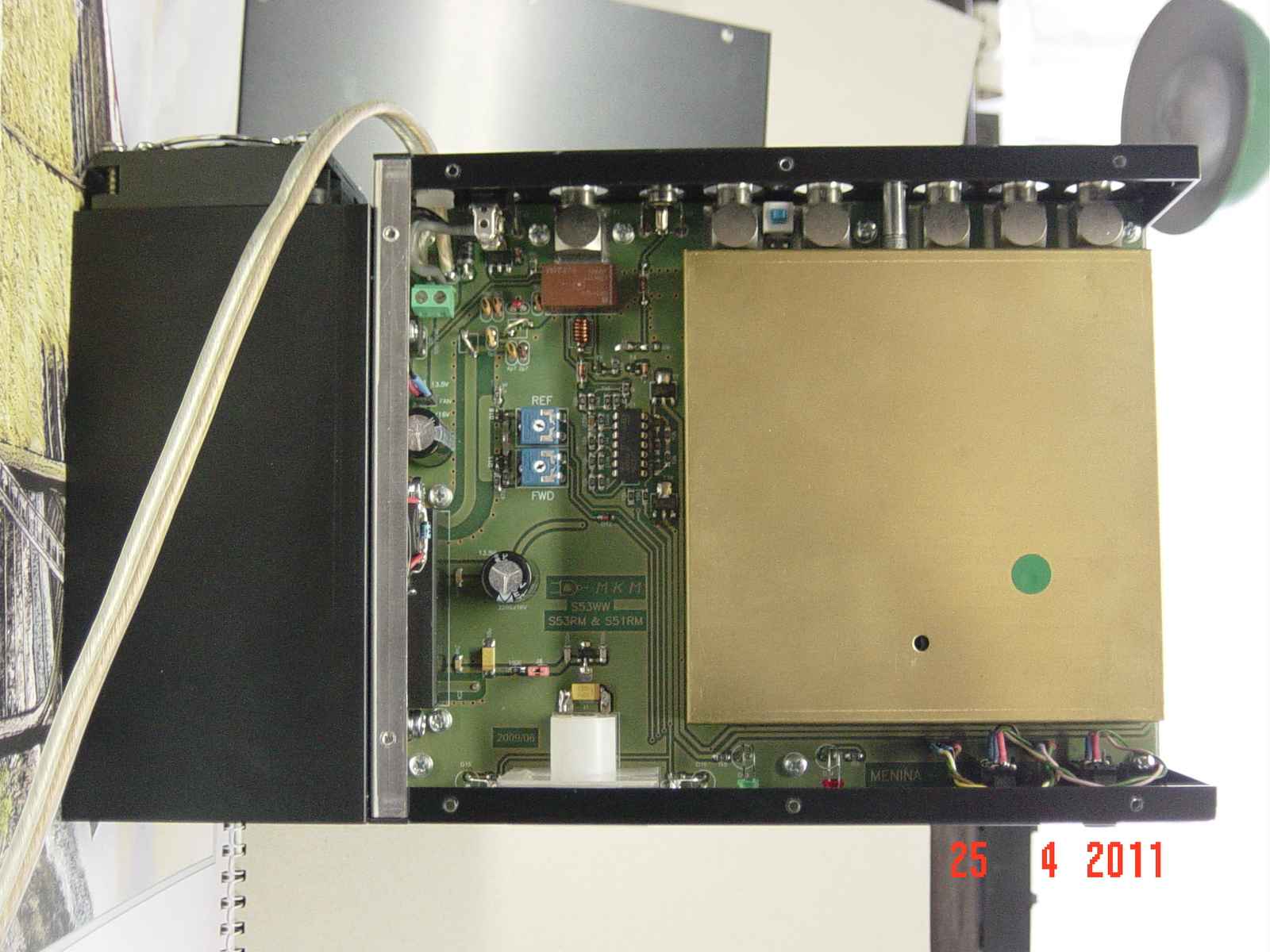
Menina II
inside with cover. |
|
|
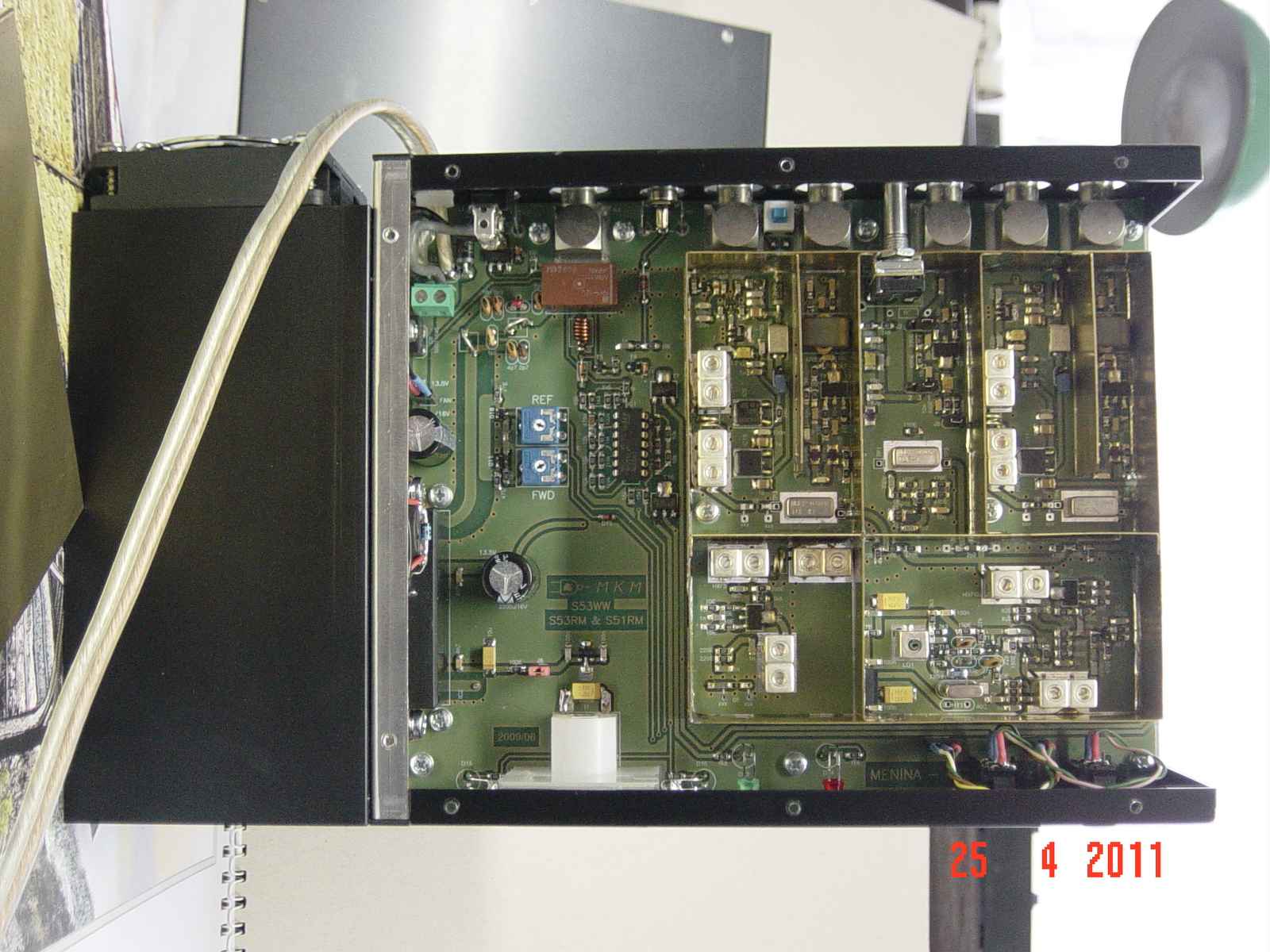
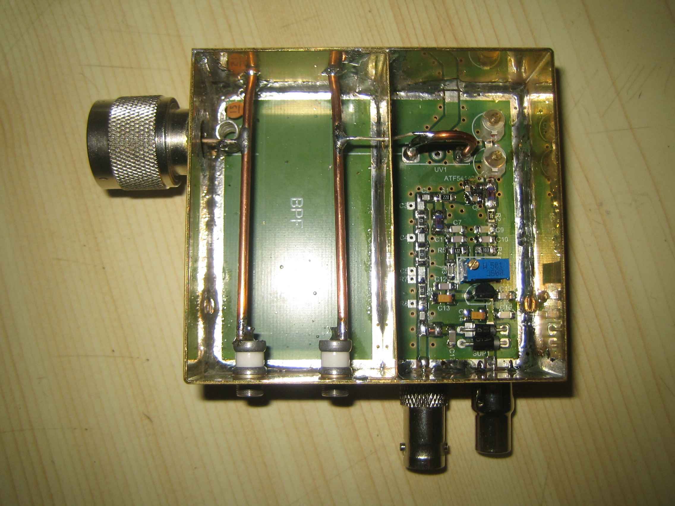
Menina II
inside. |
|
|
||||
|
|
Menina II LNA
with ATF-54143 and INPUT band pass filter and notch filter for 144 MHz. |
|
|
N – to normally open (N/O) terminal of antenna coaxial relay. BNC – RX coaxial
cable with 13V on central wire from Menina II ANT1
IN or ANT2 IN connectors. CHINCH – 13V
output for antenna relay. |
|
|
|
|
|
|
|
|
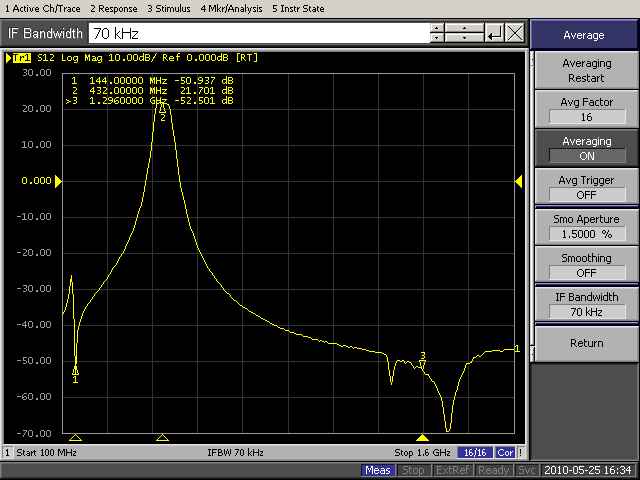
Mnina II LNA
pass band wide. |
|
|
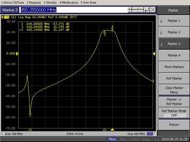
Menina II LNA
pass band narrow. |
|
|
|
|
|
|
|
|
|
|
|
|
Menina II Schematic 1, Schematic 2, LNA Schematic
Menina II PCB layout, Menina
II LNA PCB
layout
Technical data:
|
Weight |
2 kg |
|
Dimensions |
277 x 163 x 60 mm |
|
MAX. output power
for linear operation |
45W (RA45H4047M) 60W (RA60H4047M) |
|
Power
consumption |
10A @ 13,8V on TX
(45W) 0.7A @ 13,8V on RX |
|
PTT OUT max
current |
5A |
|
Max current
consumption for LNA on ANT1 IN and ANT2 IN connectors |
500mA |
|
IF IN |
-20 to +20 dBm (21 MHz) |
|
Preamplifier
(ATF-54143) |
G=20 dB, -50 dB @ 144 MHz NF=0.5 dB |
You can find more technical data on S53WW page.
73 Sine – S53RM