(ANALOG)
(DESIGN)
(MODULES)
(ASSEMBLY)
(HOME)
ARM DSP Vertical Navigation Radar
Matjaz Vidmar, S53MV
2. Modules
The ARM DSP Vertical Navigation Radar as proposed in the previous section "Design" includes many practical electronic circuits. These are grouped into six different modules built on printed-circuit boards. The detailed electrical circuit diagrams of all six modules are presented in this section. The microwave modules are very similar to the old analog Vertical Navigation Radar design.
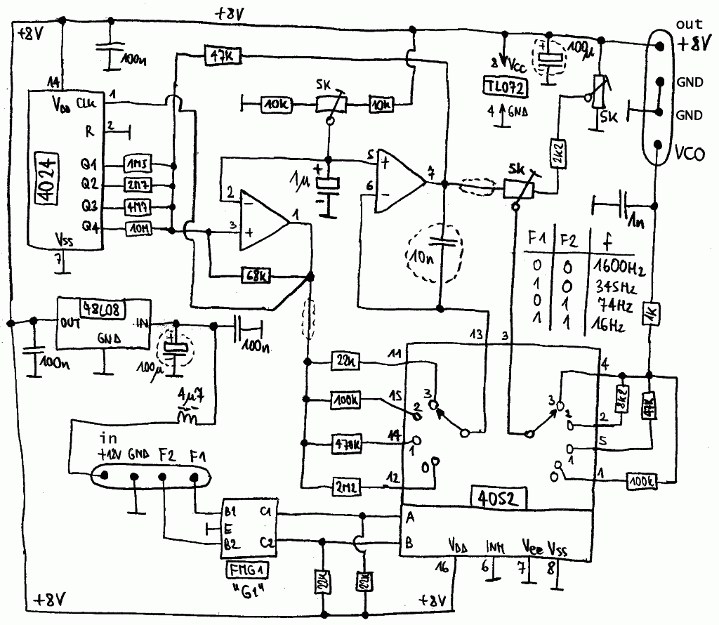
The sweep module includes a triangular-sweep generator and +8V power supply circuits for the whole transmitter. The triangular-sweep generator includes a triangular oscillator with a TL072 double operational amplifier, an analog switch CD4052 to select one out of four resistors, TTL-to-CMOS level shifters with a FMG1 dual digital transistor and a dither generator with a CD4024 binary counter.
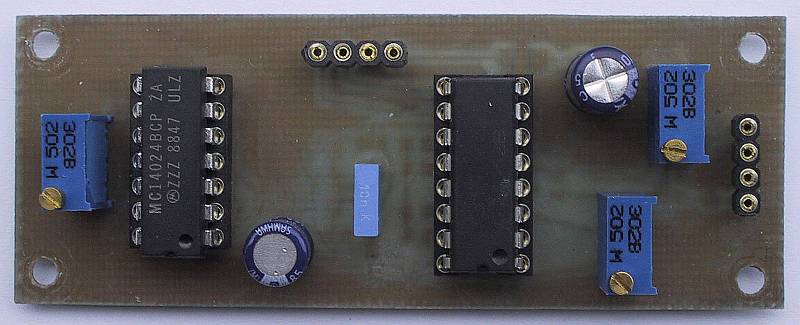
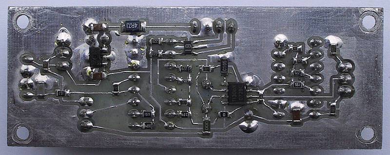
The triangular-sweep generator may generate 4 different sweep frequencies, selected with 2 TTL (3.3V) inputs. There are three trimmers to adjust the symmetry, amplitude and offset of the generated triangular sweep. The second section of the CD4052 analog switch is used for the output-signal filter, required due the power-spectrum averaging that is sensitive to switching glitches. The module is built on a single-sided PCB with the dimensions of 30mmX80mm, as shown on the following images:

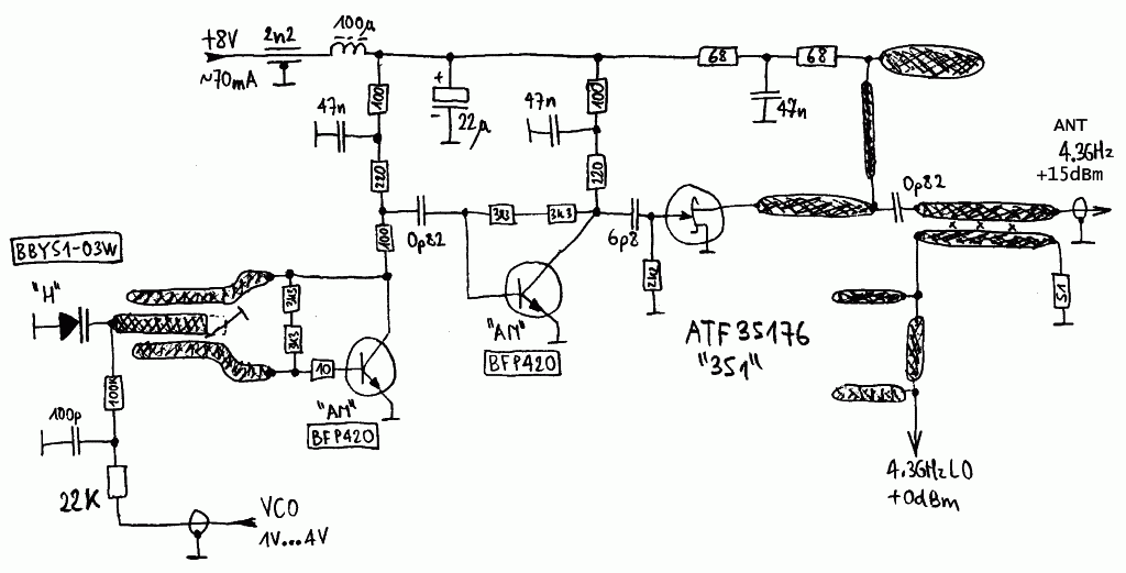
The transmitter module includes a 4.3GHz VCO (BBY51-03W and BFP420), a buffer stage (another BFP420), a power-amplifier stage (ATF35176)generating about 30mW (+15dBm) and a coupler for the receiver LO. The 20mmX80mm module is almost identical to the old design and is built in microstrip technology on a double-sided teflon laminate with a dielectric constant of 2.43 and 19mils (0.5mm) thickness, as shown on the following images:
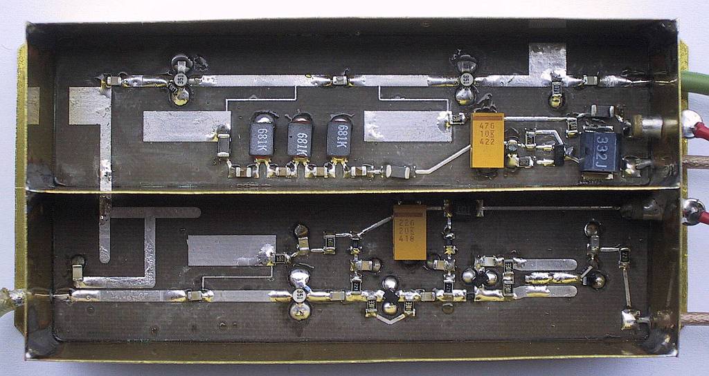
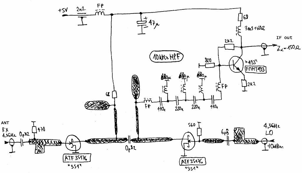
The receiver module includes a 4.3GHz LNA (ATF35176), a passive HEMT mixer stage (another ATF35176), a 10kHz high-pass filter and an IF amplifier (FMMT493). The passive HEMT mixer has an insertion loss of about 5dB, but on the other hand it handles 20dB higher signal levels and provides a 30dB wider dynamic range than the IAM81008 mixer in the old design. The 20mmX80mm module is built in microstrip technology on a double-sided teflon laminate with a dielectric constant of 2.43 and 19mils (0.5mm) thickness, as shown on the following image:
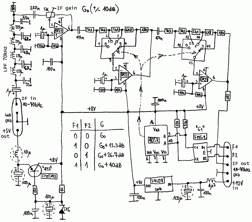
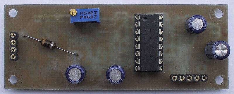
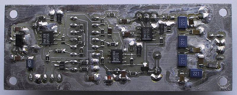
The IF module includes a lowpass filter for 70kHz, three variable-gain amplifier stages with OP27 operational amplifiers and power-supply circuits for the whole receiver chain. The gain of the first OP27 is adjusted by a trimmer to compensate for other component tolerances. The gain of the following two OP27 is switched among four different values 0dB, +13.3dB, +26.7dB and +40dB to compensate for different signal levels in different altitude ranges. The gain is switched with a CD4052 analog switch driven by a FMG1 TTL(3.3V)-to-CMOS level converter. The module is built on a single-sided PCB with the dimensions of 30mmX80mm, as shown on the following images:
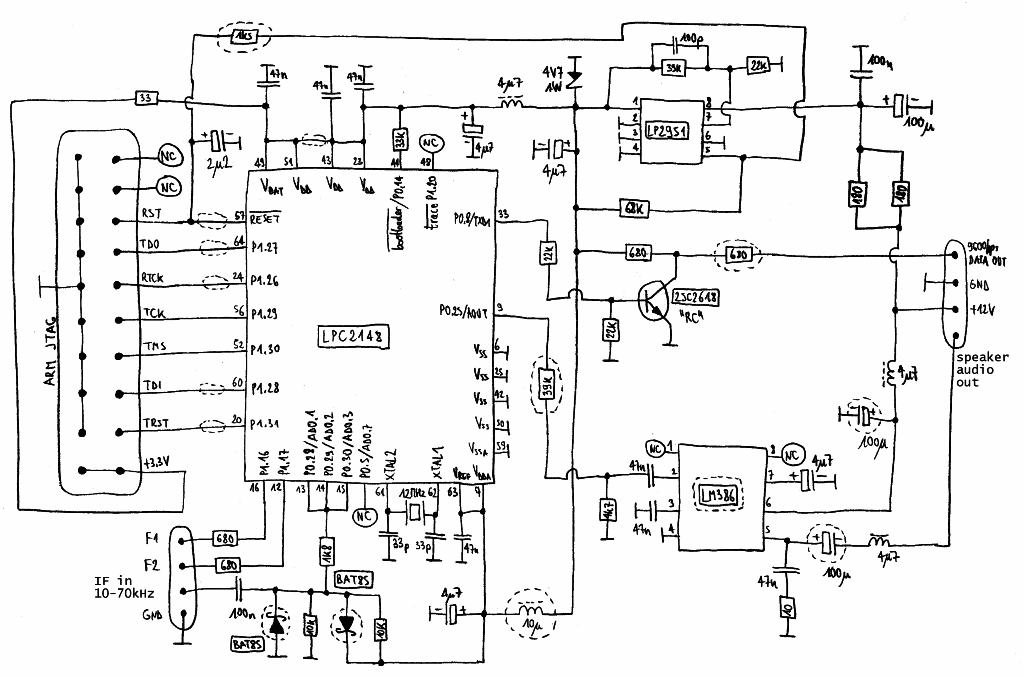
The main-processor module includes a LPC2148 ARM microcontroller and associated circuits: 12MHz clock, +3.3V power supply and reset (LP2951).
An output audio amplifier LM386 is also installed in the same module as well as a simple RS-232 driver. A standard 20-pin ARM JTAG connector is used to program the LPC2148 FLASH first and later to select some operating parameters by installing jumpers.
Since most of the signal processing is performed inside the LPC2148 (system-on-a-chip), there are just five (5) signal wires connecting the LPC2148 to other circuits: an analog input for the IF beat signal, a 9600bps RS-232 output for the graphical/numerical data, an analog output for the synthesized voice and two digital signals to switch among four sweep frequencies.
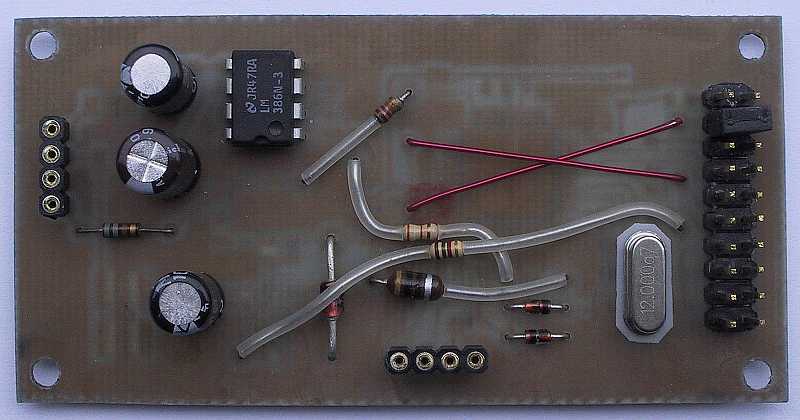
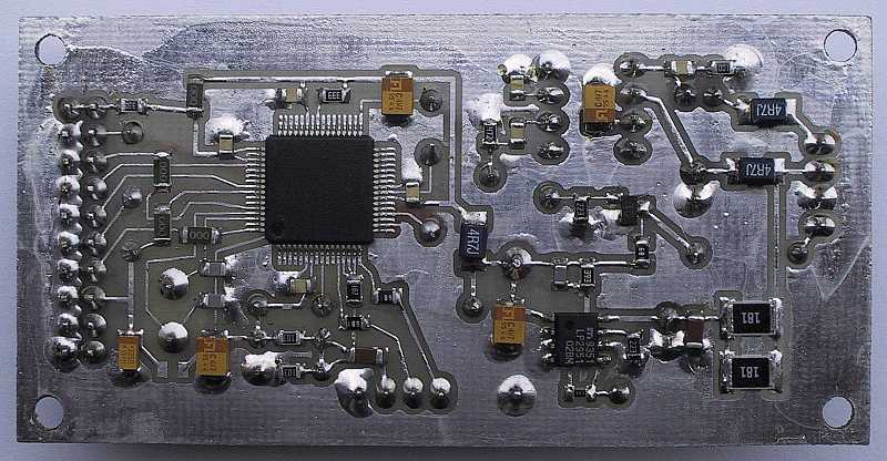
The analog input includes a bias circuit and protection diodes. The analog IF beat signal is fed to several pins of the LPC2148. In this way the FIQ (interrupt) rate can be halved to 85kHz while the input signal is sampled at 170kHz by using some internal logic of the built-in 10-bit A/D converter. The module is built on a single-sided PCB with the dimensions of 40mmX80mm, as shown on the following images:
The resources inside the LPC2148 microcontroller actually define the capabilities of the whole instrument. While the ARM core running at 60MHz is processing one segment data for 22ms, at the same time about 4ms are allocated to analog-circuit settling and 18ms are allocated to next-segment signal sampling. The 32kbyte internal RAM is allocated in the following way: 16kbytes for the 2048-FFT complex variables, 8kbytes for a fast sine/cosine lookup table for the FFT, 6kbytes for the A/D data buffer, 1kbyte for the final result averaging and just a single kilobyte remains for everything else. About 150kbytes of the internal FLASH are used by the software, mostly for recorded voice messages.
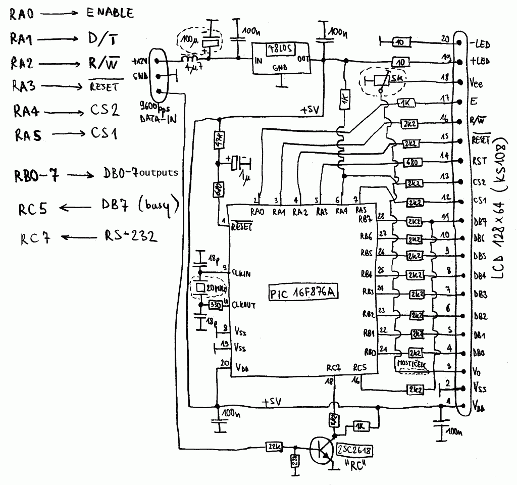
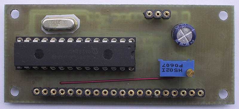
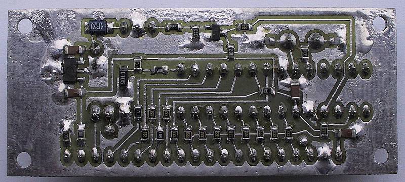
The LCD module has its own processor including a PIC 16F876A microprocessor and associated circuits: power supply, clock, reset and a RS-232 level converter. The graphical LCD module WG12864B is connected directly to the PIC16F876A. The module is built on a single-sided PCB with the dimensions of 30mmX70mm, as shown on the following images:
The installation and interconnection of the six modules is presented in the following section "Assembly".
(ANALOG) (DESIGN) (MODULES) (ASSEMBLY) (HOME)