(THEORY)
(DESIGN)
(ASSEMBLY)
(OPERATION)
(ATTENUATOR)
(HOME)
DDS RF Signal Generator
Matjaz Vidmar, S53MV
2. Design
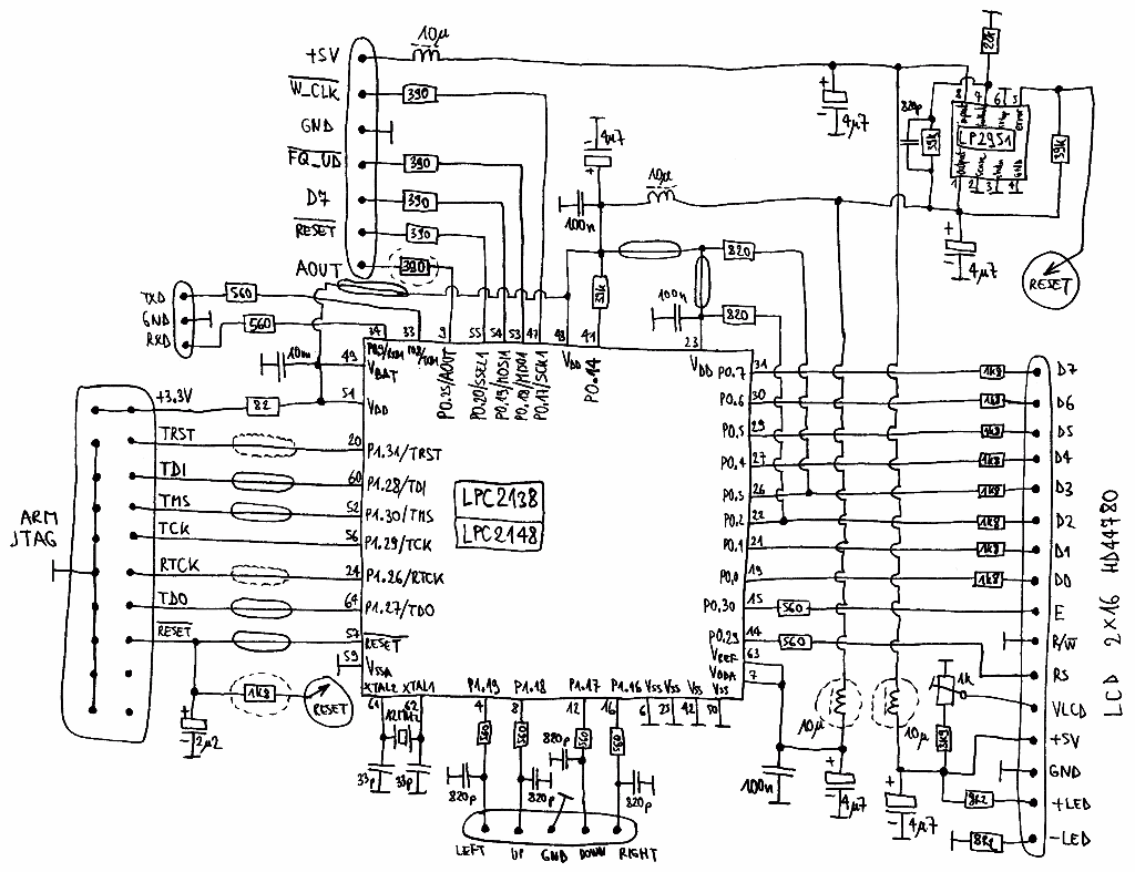
The design is split into two main modules, each built on its own printed-circuit board. The CPU board carries the LPC2138 ARM microcontroller and all associated circuits:
The LPC2138 ARM microcontroller offers comfortable 32-bit arithmetics and fast instruction execution. Most instructions only take one clock cycle or less than 17ns at a 60MHz CPU clock frequency. This represents a significant advantage over obsolete 8-bit microcontrollers that are simply too slow for this application.
The CPU module includes a 12MHz clock crystal, multiplied internally to 60MHz inside the LPC2138, reset and power-supply circuits. The module has several connectors: for the keypad (four simple switches to ground), for the LCD module, for the interface to the DDS module and power supply, for the JTAG interface used to program the microcontroller and a (spare) UART1 port. Most of the components are SMD and are installed on the solder-side of the single-sided PCB:
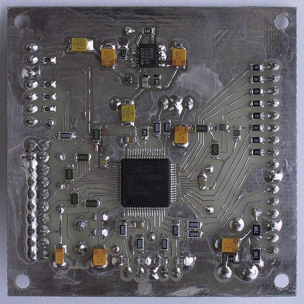
A LP2951 regulator provides both the +3.3V supply voltage and the RESET signal for the LPC2138 microcontroller. The HD44780 controller built inside the LCD module accepts 3.3V logic signals although its operating voltage is +5V. Interference-suppression resistors are used on all signal lines. Some pins of the LPC2138 require external pullups: P0.2, P0.3 and P0.14. Some JTAG programmers may require an additional pulldown resistor on the JTAG signal RTCK to enable the JTAG circuits inside the LPC2138.
The same circuit and software will also operate with the LPC2148 microcontroller. The LPC2148 has an additional USB port. The corresponding pins are left unused in this circuit to allow further expansions.
Besides the DDS chip AD9851 the second module includes a 33.333MHz clock oscillator, a lowpass filter (LM358) for amplitude modulation, a logic-level conversion stage (74ACT14) for the serial data and comprehensive supply-filtering networks:
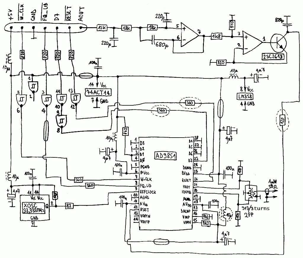
The clock frequency is multiplied by 6 to 200MHz by an internal PLL inside the AD9851. Other clock frequencies may also be used within the operating range of the AD9851. The software provides a simple menu to set the desired clock frequency and adjust accordingly all computations.
The AD9851 requires CMOS signal levels at all inputs. Since it is supplied at +5V in this project, a logic-level conversion is required for the 3.3V signals coming from the LPC2138 ARM microcontroller. A 74ACT14 is used for this purpose. In addition the built-in hysteresis inside the 74ACT14 cleans the pulses traveling along wires from the CPU module.
The first section of the LM358 performs as an anti-aliasing lowpass in AM modes. The second section of the same IC and the following 2SC2618 NPN transistor operate as a current source for the AD9851 DAC bias circuit. The 820pF capacitor on the output of the current source prevents instabilities and oscillations of the bias regulator inside the AD9851.
The DDS module includes a single connector for the interface to the CPU module and power supply. Most of the components are SMD and are installed on the solder-side of the single-sided PCB:
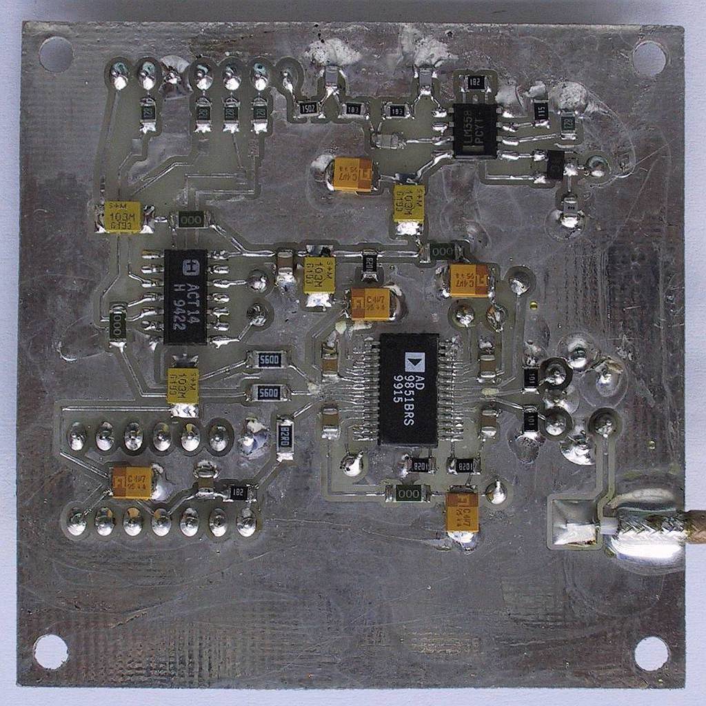
In order to obtain the highest signal-to-interference ratio, both true and complementary outputs of the AD9851 DAC are fed to a balun transformer. The RF-output cable and in particular its braid is soldered directly to the PCB to avoid shielding problems!
Both generator modules require a +5V power supply. A 7805 regulator is a simple and efficient solution. Some additional components are required for interference suppression:
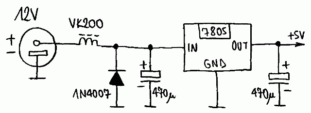
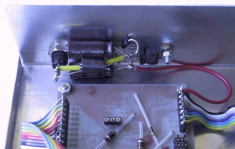
The 7805 regulator is bolted directly to the rear panel for heat-sinking:
Some older LCD modules may provide poor contrast or no display at all at a supply voltage of +5V. In this case a simple voltage doubler is required for the Vo or Vlcd voltage. The latter is referenced to the +5V supply and some modules may require it negative with respect to ground.
A simple low-current voltage doubler may be built with the 7660 chip. A similar circuit can also be built with the more popular 74HC4053 chip as shown on the following drawing:
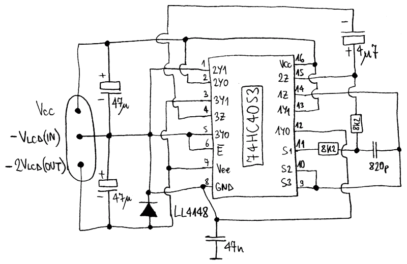
The 74HC4053 requires just a few capacitors and resistors to operate as a low-current (1mA) negative-voltage doubler. The first switch of the 74HC4053 is used as a non-inverting amplifier for the oscillator operating at around 70kHz. The second switch acts both as an inverting amplifier for the oscillator and as an output driver. Finally the third switch operates as a synchronous rectifier for the negative output voltage.
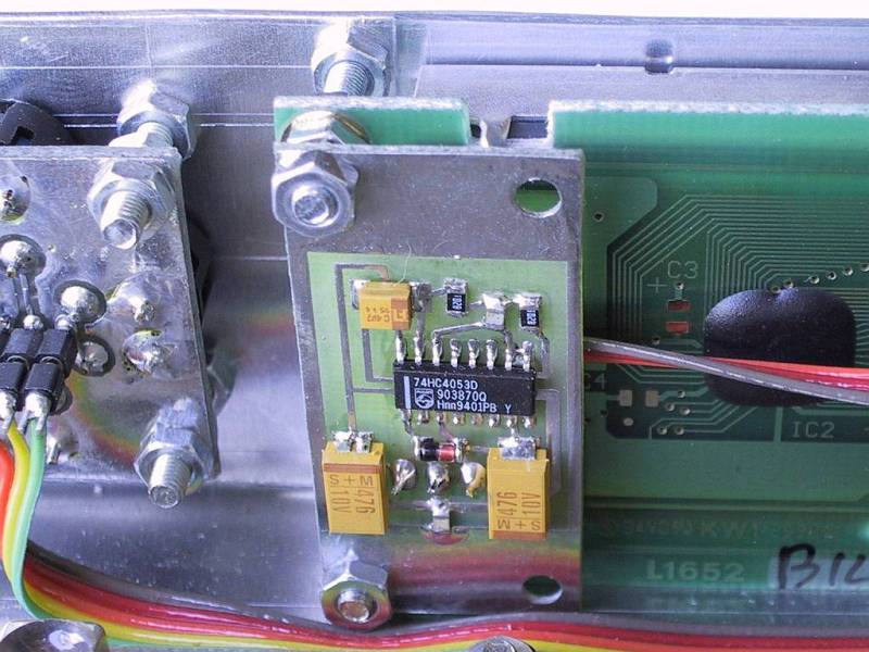
The voltage doubler is built on a small PCB bolted directly to the LCD module:
(THEORY) (DESIGN) (ASSEMBLY) (OPERATION) (ATTENUATOR) (HOME)