(THEORY)
(DESIGN)
(ASSEMBLY)
(OPERATION)
(ATTENUATOR)
(HOME)
DDS RF Signal Generator
Matjaz Vidmar, S53MV
1. Theory
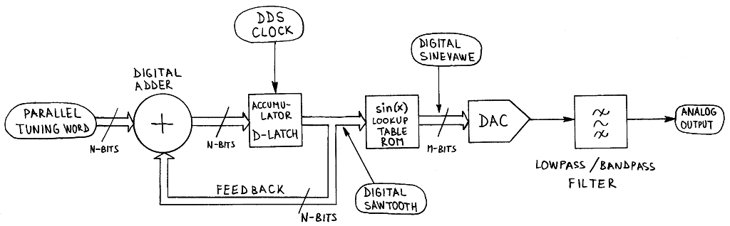
In this article a simple, modulated radio-frequency signal source is presented. Both the RF signal and the modulating waveforms are generated in a digital way. The principle of operation of a Direct Digital Synthesizer (DDS) is shown on the following drawing:
During each clock cycle, a specified number (the parallel tuning word) is added to the content of an accumulator. The content of the accumulator therefore represents a sawtooth signal whose frequency is directly proportional to the number added to the accumulator. Frequency resolution is defined by the accuracy of the mathematical operation or in other words the number N of bits used in the computations. The sawtooth signal is converted to sinewave using a ROM lookup table. Finally the digital signal is converted to analog format using a DAC.
The presented block diagram can be implemented in many different ways. For audio frequencies up to a few MHz a software implementation on a DSP processor is a simple and efficient solution. Dedicated hardware is required for higher frequencies in the radio-frequency range. Both solutions are used in this project, the former for the audio modulation and the latter for the RF carrier.
A digitally-generated sinewave includes many spectral components as shown on the following drawing taken from the AD9851 data sheet:
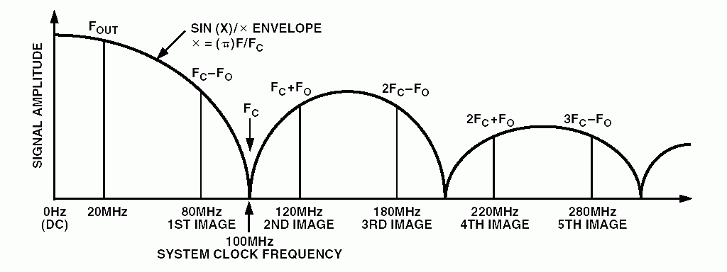
The unwanted spectral components may be attenuated by using higher clock frequencies and/or additional filtering of the output signal. On the other hand, higher-order image spectral lines can be practically used as additional signals available from the same DDS source.
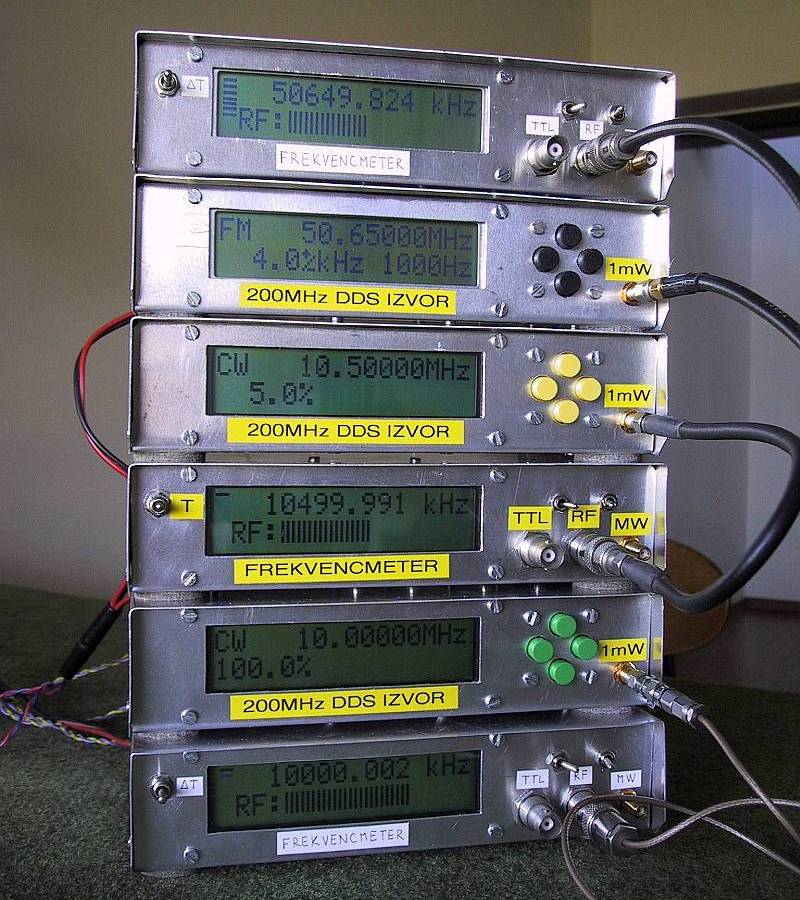
The DDS RF signal generator presented in this article is based on two chips: an AD9851 generates the RF carrier as a 200MHz DDS, while a LPC2138 ARM microcontroller performs all remaining functions operating at a clock frequency of 60MHz. Inside the LPC2138 a DSP interrupt routine running at 100kHz generates all modulation signals up to 10kHz. Further the LPC2138 accepts commands from the keypad, drives a LCD module and programs the registers inside the AD9851 through a serial interface:
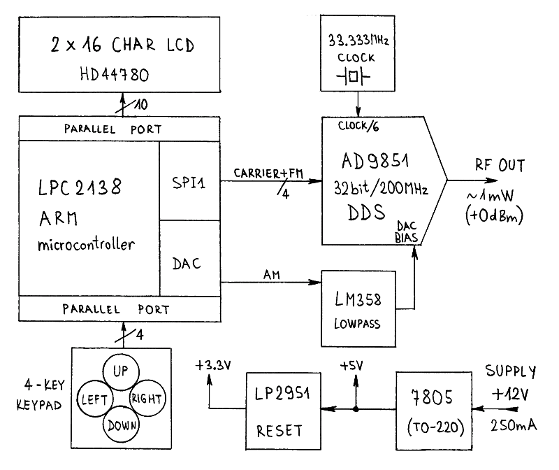
Frequency modulation is added to the digital carrier information sent to the AD9851. Since any aliasing products can not be filtered, the modulation frequency has to be kept much lower than the DSP interrupt frequency (100kHz) in FM mode.
Amplitude modulation is applied in analog way to the bias circuit of the AD9851 (carrier) DAC. An analog lowpass filter (LM358) suppresses aliasing products from the LPC2138 (modulation) DAC in AM mode.
No filtering is applied to the RF output so that all available spectral lines can be used. In order to measure communication radio receivers, an additional external adjustable attenuator of up to 120dB has to be added.
The complete DDS RF signal generator is built on two single-sided printed-circuit boards, installed in a simple aluminum enclosure:
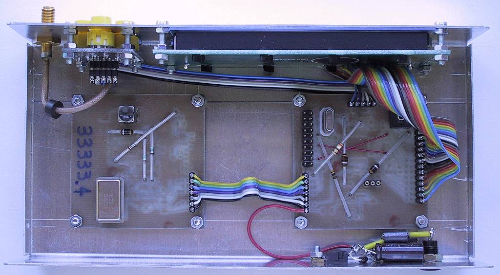
The latter provides enough shielding for receiver measurements beyond -120dBm (0.2uV) using external attenuators. The power drain of the complete instrument is about 250mA at 12V.
The performance of the instrument is mainly limited by the AD9851 DDS chip. The latter is only specified for operation up to 180MHz, although reliable operation was obtained beyond 200MHz in all three prototypes built:
The resolution of the AD9851 DAC is only M=10bits, limiting the output signal-to-interference ratio to about 60dB. Therefore the described DDS RF signal generator has some limitations. For example its output signal is not clean enough to be used for adjacent-channel interference measurements in communication receivers.
(THEORY) (DESIGN) (ASSEMBLY) (OPERATION) (ATTENUATOR) (HOME)